74LVC32A(2018) 데이터 시트보기 (PDF) - NXP Semiconductors.
부품명
상세내역
일치하는 목록
74LVC32A Datasheet PDF : 14 Pages
| |||
Nexperia
74LVC32A
Quad 2-input OR gate
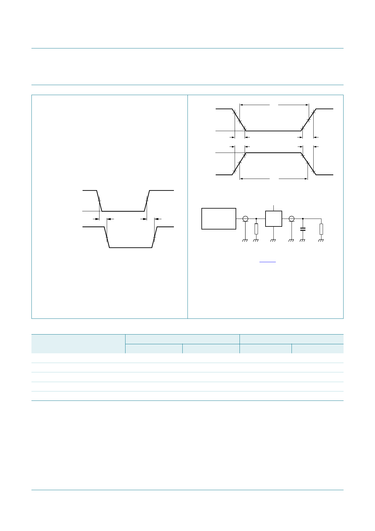
10. Dynamic characteristics
Table 7. Dynamic characteristics
Voltages are referenced to GND (ground = 0 V). For test circuit see Fig. 8.
Symbol Parameter
Conditions
-40 °C to +85 °C
Min Typ [1] Max
tpd
propagation delay nA, nB to nY; see Fig. 7
[2]
VCC = 1.2 V
-
10
-
VCC = 1.65 V to 1.95 V
0.5
4.2
9.0
VCC = 2.3 V to 2.7 V
1.5
2.4
4.9
VCC = 2.7 V
1.5
2.5
4.4
VCC = 3.0 V to 3.6 V
1.0
2.2
3.8
tsk(o) output skew time VCC = 3.0 V to 3.6 V
[3] -
-
1.0
CPD
power dissipation per gate; VI = GND to VCC [4]
capacitance
VCC = 1.65 V to 1.95 V
-
4.7
-
VCC = 2.3 V to 2.7 V
-
8.0
-
VCC = 3.0 V to 3.6 V
-
11.0
-
-40 °C to +125 °C Unit
Min
Max
-
- ns
0.5
10.4 ns
1.5
5.7 ns
1.5
5.5 ns
1.0
5.0 ns
-
1.5 ns
-
- pF
-
- pF
-
- pF
[1] Typical values are measured at Tamb = 25 °C and VCC = 1.2 V, 1.8 V, 2.5 V, 2.7 V, and 3.3 V respectively.
[2] tpd is the same as tPLH and tPHL.
[3] Skew between any two outputs of the same package switching in the same direction. This parameter is guaranteed by design.
[4] CPD is used to determine the dynamic power dissipation (PD in μW).
PD = CPD × VCC2 × fi × N + Σ(CL × VCC2 × fo) where:
fi = input frequency in MHz; fo = output frequency in MHz
CL = output load capacitance in pF
VCC = supply voltage in Volts
N = number of inputs switching
Σ(CL × VCC2 × fo) = sum of the outputs
74LVC32A
Product data sheet
All information provided in this document is subject to legal disclaimers.
Rev. 6 — 12 September 2018
© Nexperia B.V. 2018. All rights reserved
6 / 14
Share Link: 