SIT8103AI-83-28E-8.00000T 데이터 시트보기 (PDF) - Unspecified
부품명
상세내역
일치하는 목록
SIT8103AI-83-28E-8.00000T Datasheet PDF : 4 Pages
| |||
SiT8103
High Performance 1-110 MHz Oscillator
Pin Description Tables
Pin #1 Functionality
OE
H or Open[2]: specified frequency output
L: output is high impedance
ST
H or Open: specified frequency output
L: output is low level (weak pull down). Oscillation stops
Pin Map
Pin
Connection
1
OE/ST
2
GND
3
CLK
4
VDD
Absolute Maximum Table
Attempted operation outside the absolute maximum ratings of the part may cause permanent damage to the part. Actual performance of the IC
is only guaranteed within the operational specifications, not at absolute maximum ratings.
Parameter
Storage Temperature
VDD
Electrostatic Discharge
Theta JA (with copper plane on VDD and GND)
Theta JC (with PCB traces of 0.010 inch to all pins)
Soldering Temperature (follow standard Pb free soldering guidelines)
Number of Program Writes
Program Retention over -40 to 125°C, Process, VDD (0 to 3.65 V)
Min.
-65
-0.5
–
–
–
–
–
1,000+
Max.
150
4
6000
75
24
260
1
–
Unit
°C
V
V
°C/W
°C/W
°C
NA
years
Environmental Compliance
Mechanical Shock
Mechanical Vibration
Temperature Cycle
Solderability
Moisture Sensitivity Level
Parameter
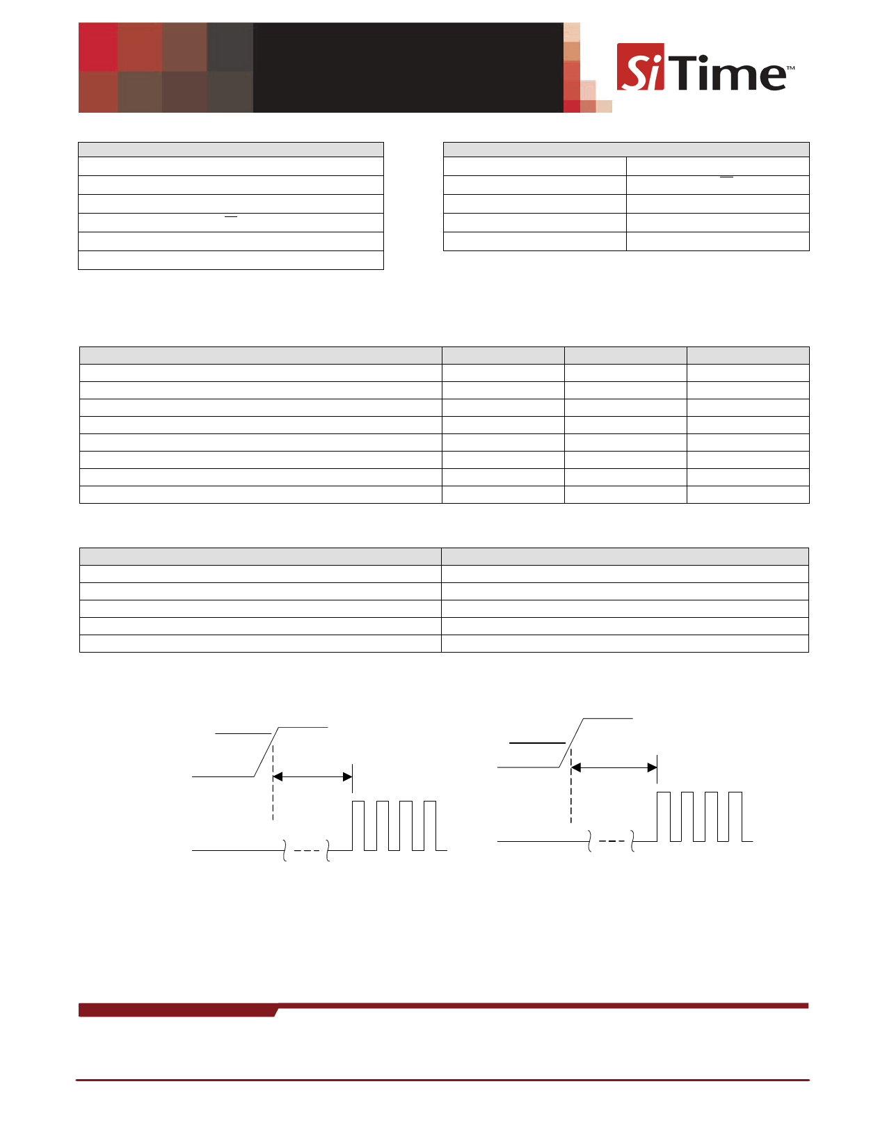
Startup and Resume Timing Diagram
Condition/Test Method
MIL-STD-883F, Method 2002
MIL-STD-883F, Method 2007
JESD22, Method A104
MIL-STD-883F, Method 2003
MSL1 @ 260°C
90% Vdd: 2.5/2.8/3.3 V parts
95% Vdd: 1.8 V parts
Vdd
Pin 4 Voltage
T_start
CLK Output
50% Vdd
Vdd
ST Voltage
T_resume
CLK Output
T_start: Time to start from power-off
(ST/OE Mode)
Note:
2. In 1.8 V mode, a resistor of <100 kΩ between OE pin and VDD is required.
T_resume: Time to resume from ST
(ST Mode Only)
■ Dimensions and Land Patterns
Rev. 1.46
Page 2 of 4
www.sitime.com
Share Link: 