A3G4250D 데이터 시트보기 (PDF) - STMicroelectronics
부품명
상세내역
일치하는 목록
A3G4250D Datasheet PDF : 44 Pages
| |||
Block diagram and pin description
A3G4250D
Table 2. Pin description
Pin#
Name
Function
1
Vdd_IO Power supply for I/O pins
SCL
I2C serial clock (SCL)
2
SPC
SPI serial port clock (SPC)
SDA
I2C serial data (SDA)
3
SDI
SPI serial data input (SDI)
SDO
3-wire interface serial data output (SDO)
SDO
SPI serial data output (SDO)
4
SA0
I2C least significant bit of the device address (SA0)
SPI enable
5
CS
I2C/SPI mode selection (1: SPI idle mode / I2C communication
enabled; 0: SPI communication mode / I2C disabled)
6
DRDY/INT2 Data ready/FIFO interrupt
7
INT1
Programmable interrupt
8
Reserved Connect to GND
9
Reserved Connect to GND
10
Reserved Connect to GND
11
Reserved Connect to GND
12
Reserved Connect to GND
13
GND
0 V supply
14
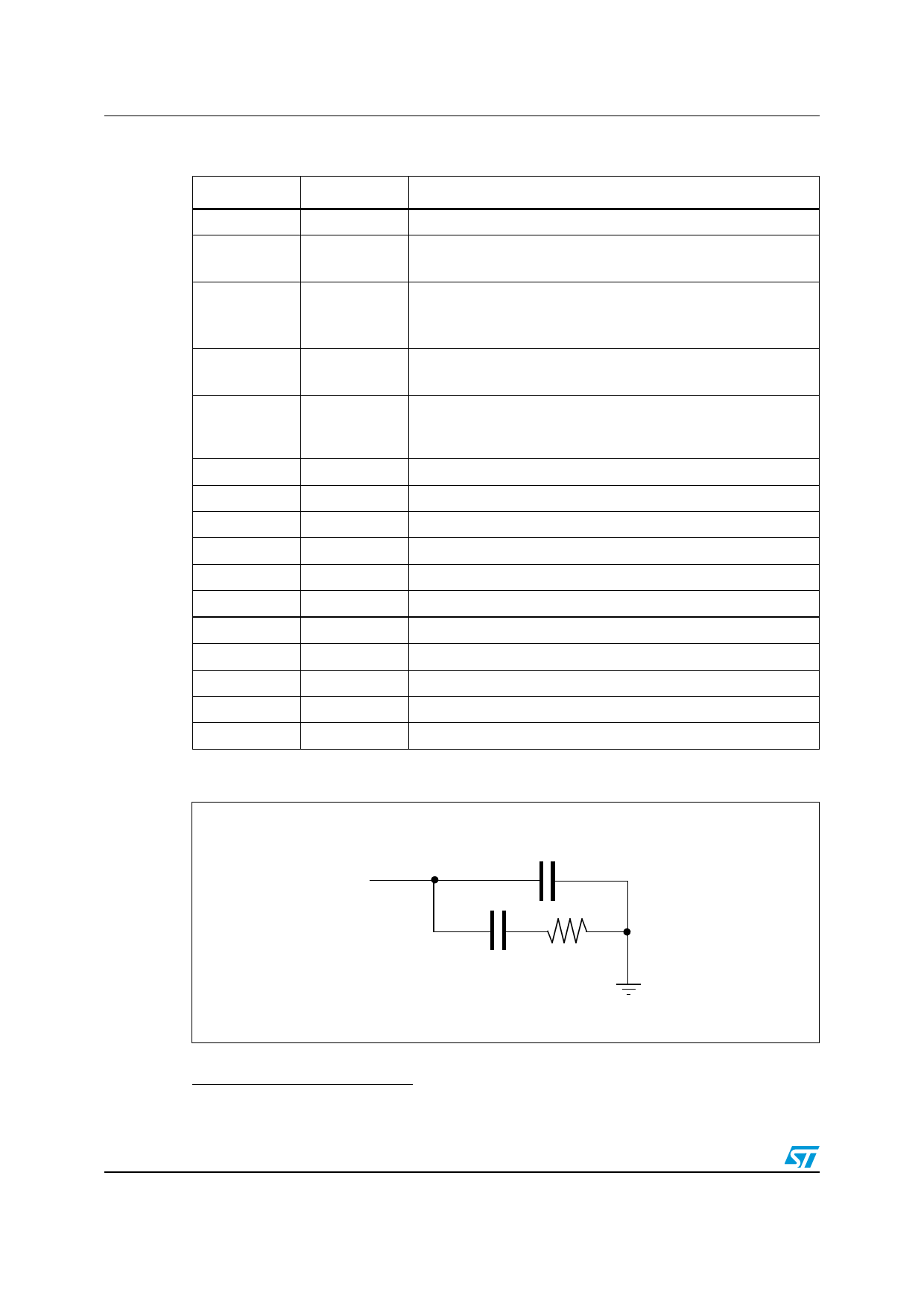
PLLFILT Phase-locked loop filter (see Figure 3)
15
Reserved Connect to Vdd
16
Vdd
Power supply
Figure 3.
A3G4250D external low-pass filter values(a)
#APACITOR�FOR�
,OWPASS�FILTER
TO�PIN�
#
#
2
'.$
!-V
8/44
a. Pin 14 PLLFILT maximum voltage level is equal to Vdd.
Doc 022768 Rev 3
Share Link: 