SCY99079CDR2G 데이터 시트보기 (PDF) - ON Semiconductor
부품명
상세내역
일치하는 목록
SCY99079CDR2G Datasheet PDF : 28 Pages
| |||
DAP018A/B/C/D/F
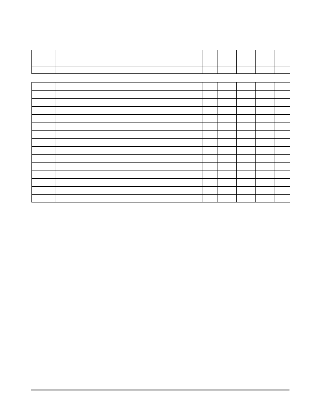
ELECTRICAL CHARACTERISTICS
(For typical values TJ = 25°C, for min/max values TJ = −25°C to +125°C, Max TJ = 150°C, VCC = 12 V unless otherwise noted)
INTERNAL RAMP COMPENSATION
Symbol
Rating
Pin Min
Typ
Max Unit
Vramp Internal ramp level @ 25°C (Note 2)
Rramp Internal ramp resistance to CS pin (Note 2)
PROTECTIONS
7
3.0
V
7
20
kW
Symbol
Rating
Pin Min
Typ
Max Unit
Vlatch
Tlatch−del
VtimFault
Itim
TimerL
Latching level input
Delay before latch confirmation
Timer level completion
Timer capacitor charging current
Timer length, Ctimer = 0.22 mF typical
2
2.85
3
3.25
V
−
20
ms
3
4.3
V
3
12
mA
3
100
ms
VBO
IBO
IBO
IBObias
TBO−del
IOTP
VOTP
TSD
Brown−Out level – B & D versions
Hysteresis current, Vpin 11 < VBO – B & D versions, TJ = 25°C
Hysteresis current, Vpin 11 < VBO – B & D versions, −25°C < TJ < 25°C
Brown−Out input bias current – B & D versions
Delay before brown−out confirmation
Over temperature shutdown current (Note 3)
Over temperature latching voltage (Note 3)
Temperature shutdown
11
0.95
1
1.05
V
11
9
10
11
mA
11
8.6
10
11
mA
11
0.02
mA
−
20
ms
12
101
113
124
mA
12 0.95
1
1.05
V
−
140
°C
TSD_hys Temperature shutdown hysteresis
−
40
°C
1. See characterization table for linearity over negative bias voltage.
2. Guaranteed by design.
3. The OTP parameters are selected to cope with a TTC03−474 which offers a resistance of 8.8 kW when heated to a temperature of 110°C.
4. The brown−out circuitry is disabled on versions A & C and operates on versions B & D.
http://onsemi.com
7
Share Link: 