SCY99079ADR2G 데이터 시트보기 (PDF) - ON Semiconductor
부품명
상세내역
일치하는 목록
SCY99079ADR2G Datasheet PDF : 28 Pages
| |||
DAP018A/B/C/D/F
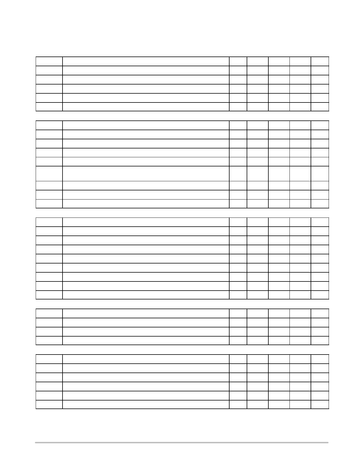
ELECTRICAL CHARACTERISTICS
(For typical values TJ = 25°C, for min/max values TJ = −25°C to +125°C, Max TJ = 150°C, VCC = 12 V unless otherwise noted)
DRIVE OUTPUT
Symbol
Rating
Pin Min
Typ
Max Unit
Tf
Output voltage fall−time @ CL = 1 nF, 10−90% of a 12 V output signal
Isource Source current capability at VDRV = 10.5 V
Isink Sink current capability at VDRV = 0 V
VDRVlow DRV pin level at VCC close to VCC(min) with a 33 kW resistor to GND
VDRVhigh DRV pin level at VCC = 28 V
CURRENT COMPARATOR
9
−
25
−
ns
9
−
500
−
mA
9
−
800
−
mA
9
7.6
−
−
V
9
10
15
17
V
Symbol
Rating
Pin Min
Typ
Max Unit
IIB
VLimit
TDEL
TLEB
TSS
Input Bias Current @ 0.8 V input level on pin 7
Maximum internal current setpoint – pin1 grounded
Propagation delay from current detection to gate off−state
Leading Edge Blanking Duration
Internal soft−start duration activated upon startup, auto−recovery and BO
release for versions B & D, pin 1 grounded.
7
0.02
mA
7
0.76
0.8
0.84
V
7
100
150
ns
7
140
ns
−
5
ms
IOPPo Setpoint decrease for pin 1 biased to –300 mV (Note 1)
1
37.5
%
IOOPv Voltage setpoint for pin 1 biased to −300 mV (Note 1)
1
0.46
0.5
0.54
V
IOPPs Setpoint decrease for pin 1grounded
1
0
%
INTERNAL OSCILLATOR
Symbol
Rating
Pin Min
Typ
Max Unit
fOSC
fOSC
Dmax
fjitter
fswing
ICjit
Oscillation frequency (65 kHz version, A & B)
Oscillation frequency (100 kHz version, C & D)
Maximum duty−cycle
Frequency jittering in percentage of fOSC
Swing frequency with a 22 nF capacitor to pin 4
Jittering modulator charging current
−
60
65
70
kHz
−
92
100
108 kHz
−
76
80
84
%
−
±5
%
4
300
Hz
4
18
mA
VCjitP Jittering capacitor peak voltage
4
2.2
V
VCjitV Jittering capacitor valley voltage
4
0.8
V
FEEDBACK SECTION
Symbol
Rating
Pin Min
Typ
Max Unit
Rup
Internal pull−up resistor
RFB
Equivalent resistor on FB pin
Iratio Pin 6 to current setpoint division ratio
FREQUENCY FOLDBACK
6
20
kW
16
kW
−
4.2
kW
Symbol
Rating
Pin Min
Typ
Max Unit
Ifold
Internal foldback reference current
5
8.5
10
11.5
mA
Vfold Frequency folback level with a 100 kW resistor to ground
5
1
V
Iskip
Skip current in percentage of the maximum excursion, for Vfold = 1 V
30
%
Ftrans Transition frequency below which skip−cycle occurs for TJ = 25°C
–
21
25
29
kHz
Vskip Skip−cycle level voltage on the feedback pin
6
320
mV
1. See characterization table for linearity over negative bias voltage.
2. Guaranteed by design.
3. The OTP parameters are selected to cope with a TTC03−474 which offers a resistance of 8.8 kW when heated to a temperature of 110°C.
4. The brown−out circuitry is disabled on versions A & C and operates on versions B & D.
http://onsemi.com
6
Share Link: 