SCY99079ADR2G 데이터 시트보기 (PDF) - ON Semiconductor
부품명
상세내역
일치하는 목록
SCY99079ADR2G Datasheet PDF : 28 Pages
| |||
Vbulk
OVP
ROPPL
+
DAP018A/B/C/D/F
ROPPU
*See
1
14
Note
2
13
3
12
4
11 NC /
5
10 A&C
6
9
7
8
Ramp
+
OTP
+
Vout
Gnd
*This resistor
prevents from
negatively biasing
the HV pin (14) at
power−off. Typical
value is 4.7 kW.
Foldback Timer Freq.
Adj. Delay Jitter
Gnd
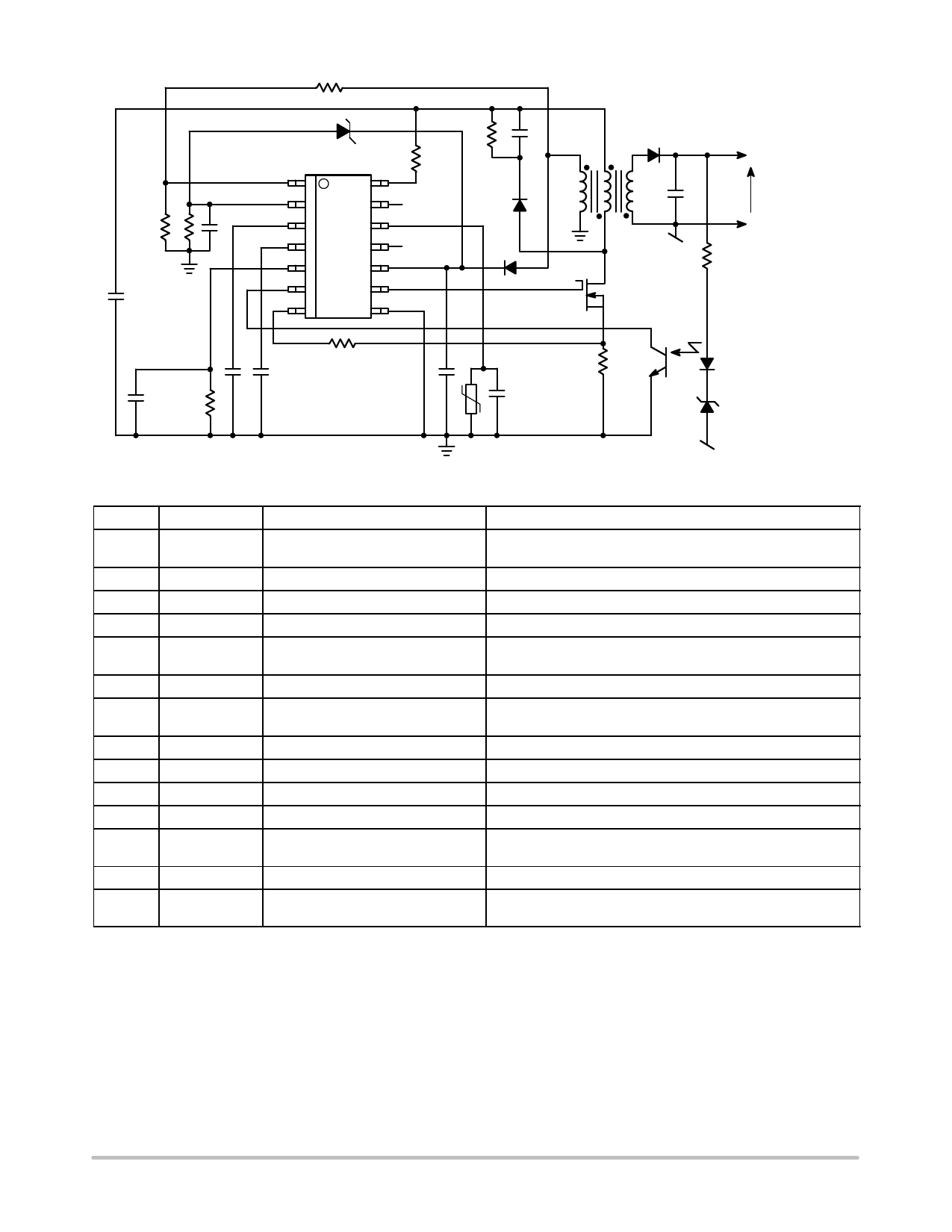
Figure 1. Typical Application Example
Pin No.
1
Pin Name
OPP
Function
Adjust the Over Power Protection
2
OVP
Input voltage to latch comparator
3
CTimer
Timer
4
Jitter
Frequency jittering speed
5
Foldback / skip Frequency foldback /
skip cycle adjustment
6
FB
Feedback pin
7
CS
Current sense +
ramp compensation
8
GND
−
9
DRV
Driver output
10
VCC
Supplies the controller
11
BO
Brown−out, B and D versions
12
OTP
NTC connection
13
NC
−
14
HV
High−voltage input
Pin Description
A resistive divider from the auxiliary winding to this pin sets the
OPP compensation level.
This pin offers an over−voltage protection input.
Wiring a capacitor to ground helps selecting the timer duration.
This pin offers a way to adjust the frequency modulation pace.
By connecting a resistor to ground, it becomes possible to re-
duce the level at which frequency foldback occurs.
Hooking an optocoupler collector to this pin will allow regulation.
This pin monitors the primary peak current but also offers a
means to introduce ramp compensation.
The controller ground.
The driver’s output to an external MOSFET gate.
This pin is connected to an external auxiliary voltage.
For B and D versions, this pin offers a brown−out input.
This pin connects to a pulldown NTC resistor for over temperat-
ure protection (OTP).
Non−connected for improved creepage.
Connected to the bulk capacitor, this pin powers the internal
current source to deliver a startup current.
http://onsemi.com
2
Share Link: 