SCY99079ADR2G 데이터 시트보기 (PDF) - ON Semiconductor
부품명
상세내역
일치하는 목록
SCY99079ADR2G Datasheet PDF : 28 Pages
| |||
DAP018A/B/C/D/F
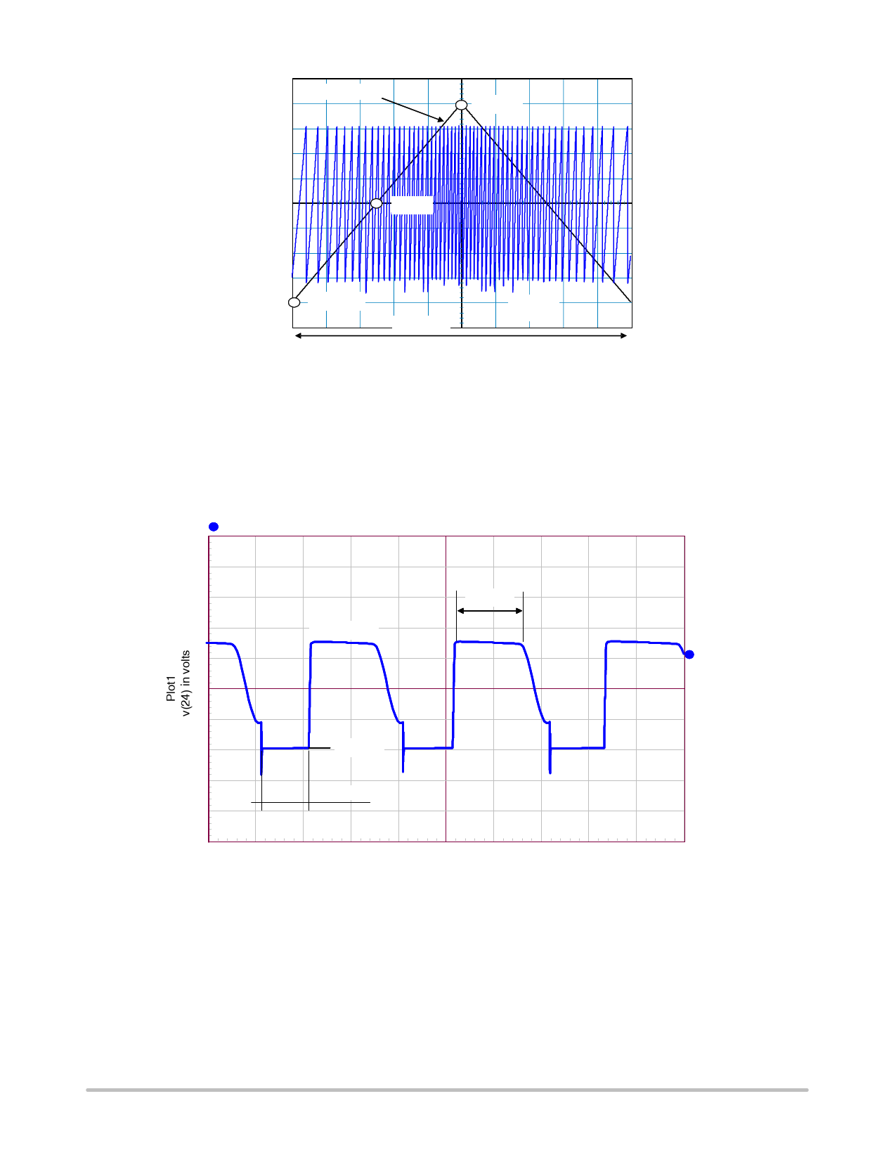
Jitter ramp
68.9kHz
65kHz
61.1kHz
adjustable
Internal
sawtooth
Figure 50. Modulation Effects on the Clock Signal by the Jittering Sawtooth
Over Power Protection
There are several known ways to implement Over Power
Protection (OPP), all suffering from particular problems.
These problems range from the added consumption burden
on the converter or the skip−cycle disturbance brought by
the current−sense offset. A way to reduce the power
capability at high line is described by Figure 52. On this
drawing, a voltage is derived from the auxiliary winding and
produces a negative level during the on−time of the main
power transistor. The negative voltage amplitude directly
relates to the input level via the transformer turn ratio linking
the primary winding to the auxiliary winding. Figure 51
depicts the typical signal obtained on the auxiliary winding:
1 v(24)
40.0
off−time
20.0
N1(Vout + Vf)
1
0
−20.0
−N2Vbulk
−40.0
on−time
464u
472u
480u
time in seconds
488u
496u
Figure 51. The Signal Obtained on the Auxiliary Winding Swings Negative During the On−time
During the off−time, the voltage plateaus to a positive
level depending on the turn ratio between the output winding
(Ns) and the power winding. This ratio is noted N1. During
the on−time, the transformer terminal swings to a negative
voltage whose amplitude now depends on the turn ratio N2,
equal to the primary (Np) to the auxiliary winding ratio
(Naux). If we place a resistive divider between the auxiliary
winding and the OPP pin, as suggested by Figure 52, we
have a means to influence the internal setpoint as the bulk
voltage increases. The equations to design the network are
fairly simple:
Suppose we need to reduce the peak current from 2.5 A at
low line, to 2 A at high line. This corresponds to 20%
reduction or a setpoint voltage of 640 mV. To reach this
level, then the negative voltage developed on the OPP pin
must reach:
VOPP + 800 * 640 + −160 mV
(eq. 4)
http://onsemi.com
25
Share Link: 