SCY99079ADR2G 데이터 시트보기 (PDF) - ON Semiconductor
부품명
상세내역
일치하는 목록
SCY99079ADR2G Datasheet PDF : 28 Pages
| |||
DAP018A/B/C/D/F
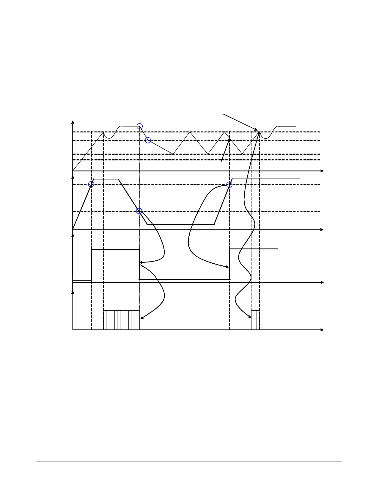
When the input voltage is low, below VBO(on), the BO
comparator output is low and the current source is activated,
drawing 10 mA from the BO pin (pin 11) to ground. The
controller is silent, and no driving pulses are delivered to the
power MOSFET. When the input is sufficiently high, the BO
comparator toggles high and shuts down the current source,
providing the necessary hysteresis to the circuit. When
toggling high, the BO signal also resets ALL the internal
logic circuits including an eventual latch state triggered by
an OVP for instance (or a latched OCP for this particular
version). When the BO comparator has given the
authorization to work, the controller resets its hiccup mode
on the VCC (if any) and waits for the next VCC(on) event to
start pulsing again (via soft−start sequence). A 20 ms RC
time−constant has been added in series with the brown−out
comparator to further avoid false trigger of the controller.
Figure 44 shows typical signals in presence of a
brown−out suddenly occuring and coming back again:
VCC
VCC(on)
VCC(min)
VCClatch
VCCreset
Vbulk
Controller waits for
the next VCC(on) event
Double hiccup 1
restart
BO acknowledged
here: hiccup reset
VBO(on)
Mains
Interruption
VBO(off)
BO
signal
General
internal reset
(latch...)
Drv
Figure 44. A Brown−out Event Immediately Stops the Driving Pulses
When the bulk comes back to its normal level, the controller waits for the next VCC(on) event to re−start pulsing. If the
controller was in a double−hiccup mode, the logic circuit is reset to accelerate the restart to the next VCC(on) event.
http://onsemi.com
21
Share Link: 