MAX2027 데이터 시트보기 (PDF) - Maxim Integrated
부품명
상세내역
일치하는 목록
MAX2027 Datasheet PDF : 10 Pages
| |||
IF Digitally Controlled Variable-Gain Amplifier
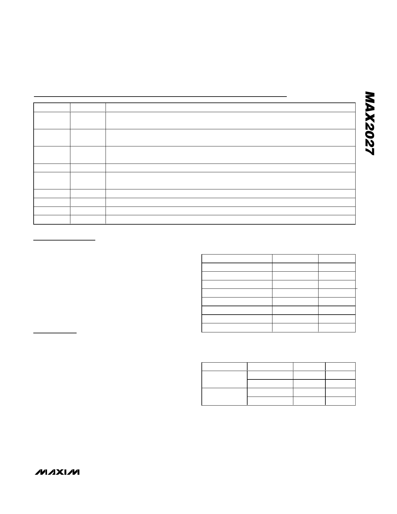
Pin Description
PIN
1, 2, 11
3
4, 5, 16, 17,
19, 20, EP
6–10
12
13
14
15
18
NAME
VCC
RF_IN
GND
B4–B0
RF_OUT
ISET
IBIAS
AMPIN
ATTNOUT
FUNCTION
Power Supply. Bypass to GND with capacitors as close to the pin as possible as shown in the typical
application circuit (Figure 1).
Signal Input. See the typical application circuit for recommended component values. Requires an
external DC-blocking capacitor.
Ground. Use low-inductance layout techniques on PC board. Solder the exposed pad evenly to the
board ground plane.
Gain-Control Bits. See Table 3 for gain setting.
Signal Output. Requires an external pullup choke inductor (52mA typical current) to VCC along with a
DC-blocking capacitor (Figure 1).
Connect an 825Ω resistor from ISET to GND.
Amplifier Bias. Connect to AMPIN (pin 15) through a choke inductor (0.3mA typ).
Amplifier Input. Requires a DC-coupling capacitor to allow biasing.
Attenuator Output. Requires an external DC-blocking capacitor.
Detailed Description
The MAX2027 is a high-performance, digitally con-
trolled variable-gain amplifier for use in applications
from 50MHz to 400MHz.
The MAX2027 incorporates a digital attenuator with a
23dB selectable attenuation range followed by a fixed-
gain, high-linearity amplifier. The attenuator is digitally
controlled through five logic lines: B0–B4. This on-chip
attenuator provides up to 23dB of attenuation with
±0.05dB state-to-state accuracy. The fixed-gain amplifi-
er utilizes negative feedback to achieve high stability,
gain, linearity, and wide bandwidth.
Applications Information
Input and Output Matching
The MAX2027 incorporates on-chip input and output
matching for operation below 250MHz. Use a DC-block-
ing capacitor value of 1000pF for pins 3, 12, and 18 (see
Figure 1). For operation above 250MHz, external match-
ing improves performance. Table 1 and Table 2 provide
recommended components for device operation.
Digitally Controlled Attenuator
The digital attenuator is controlled through five logic
lines: B0, B1, B2, B3, and B4. Table 3 lists the attenua-
tion settings. The input and output of this attenuator
require external DC-blocking capacitors. This attenua-
tor insertion loss is 2dB when the attenuator is set to
0dB (B0 = B1 = B2 = B3 = B4 = 0).
Table 1. Suggested Components of
Typical Application Circuit
COMPONENT
C1, C3, C4
C2, C5
C6, C7
C10
R1
R2–R6
L1
L2
VALUE
1000pF
100pF
0.1µF
0.047µF
825Ω ±1%
47kΩ
330nH
680nH
SIZE
0603
0603
0603
0603
0603
0603
0805
1008
Table 2. Suggested Matching
Components
FREQUENCY
300MHz
400MHz
COMPONENT
L3, L4
C8, C9
L3, L4
C8, C9
VALUE
11nH
6.8pF
8.7nH
5pF
SIZE
0603
0603
0603
0603
_______________________________________________________________________________________ 7
Share Link: 