MAX2027 데이터 시트보기 (PDF) - Maxim Integrated
부품명
상세내역
일치하는 목록
MAX2027 Datasheet PDF : 10 Pages
| |||
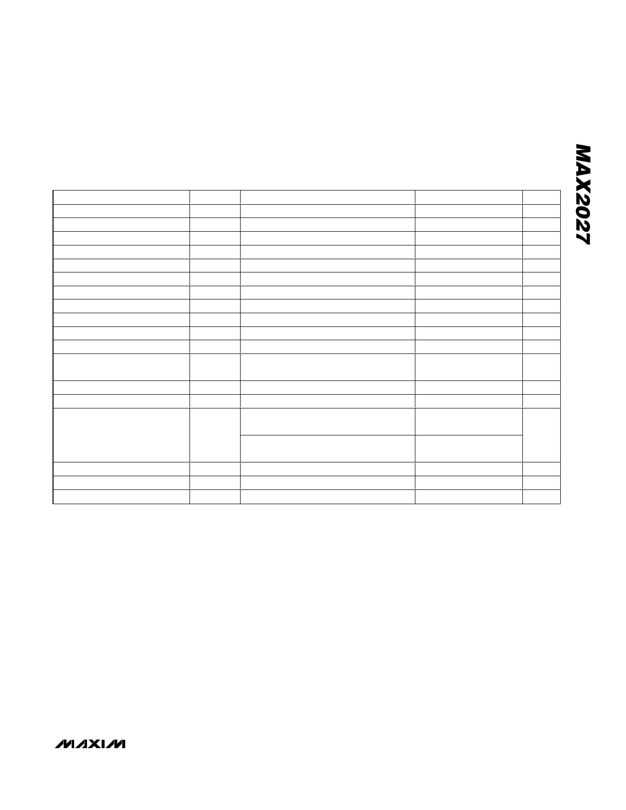
IF Digitally Controlled Variable-Gain Amplifier
AC ELECTRICAL CHARACTERISTICS
(Typical application circuit without matching, VCC = +4.75V to +5.25V, GND = 0V, max gain (B0 = B1 = B2 = B3 = B4 = 0), R1 =
825Ω, POUT = 5dBm, fIN = 50MHz, 50Ω RF system impedance. Typical values are at VCC = +5V and TA = +25°C, unless otherwise
noted.) (Notes 1, 2)
PARAMETER
SYMBOL
CONDITIONS
MIN TYP MAX UNITS
Frequency Range
Gain
Noise Figure
fR
G
No attenuation
NF
Max gain
50
400 MHz
15.5
dB
4.7
dB
Minimum Reverse Isolation
Max gain
22
dB
Output 1dB Compression Point
P1dB Max gain
20.6
2nd-Order Output Intercept Point
OIP2 f1 + f2, f1 = 50MHz, f2 = 51MHz, 5dBm/tone
42
3rd-Order Output Intercept Point
OIP3 All gain conditions, 5dBm/tone
34.7
dBm
dBm
dBm
2nd Harmonic
2fIN
3rd Harmonic
3fIN
RF Gain-Control Range
-44
dBc
-68
dBc
23
dB
Gain-Control Resolution
1
dB
Attenuation Absolute Accuracy
Compared to the ideal expected
attenuation
0.15/
-0.05
dB
Attenuation Relative Accuracy
Between adjacent states
±0.05
dB
Gain Drift Over Temperature
TA = -40°C to +85°C
±0.1
dB
Gain Flatness Over 50MHz BW
Attenuator Switching Time
Peak-to-peak for all settings,
FCENTER = 75MHz
Peak-to-peak for all settings,
FCENTER = 200MHz
50% control to 90% RF
0.1
dB
0.2
40
ns
Input Return Loss
Output Return Loss
fR = 50MHz to 250MHz, all gain conditions
15
dB
fR = 50MHz to 250MHz, all gain conditions
15
dB
Note 1: Guaranteed by design and characterization.
Note 2: All limits reflect losses of external components. Output measurements are taken at RF OUT using the typical application
circuit.
_______________________________________________________________________________________ 3
Share Link: 