AN-9719 데이터 시트보기 (PDF) - Fairchild Semiconductor
부품명
상세내역
일치하는 목록
AN-9719 Datasheet PDF : 12 Pages
| |||
AN-9719
One simple and practical way to address this problem is
designing the feedback loop for low input voltage and full-
load condition with enough phase and gain margin. When
the converter operates in CCM, the RHP zero is lowest in
low input voltage and full-load condition. The gain
increases only about 6dB as the operating condition is
changed from the lowest input voltage to the highest input
voltage condition under universal input condition. When the
operating mode changes from CCM to DCM, the RHP zero
disappears, making the system stable. Therefore, by
designing the feedback loop with more than 45 degrees of
phase margin in low input voltage and full-load condition,
the stability over all the operating ranges can be guaranteed.
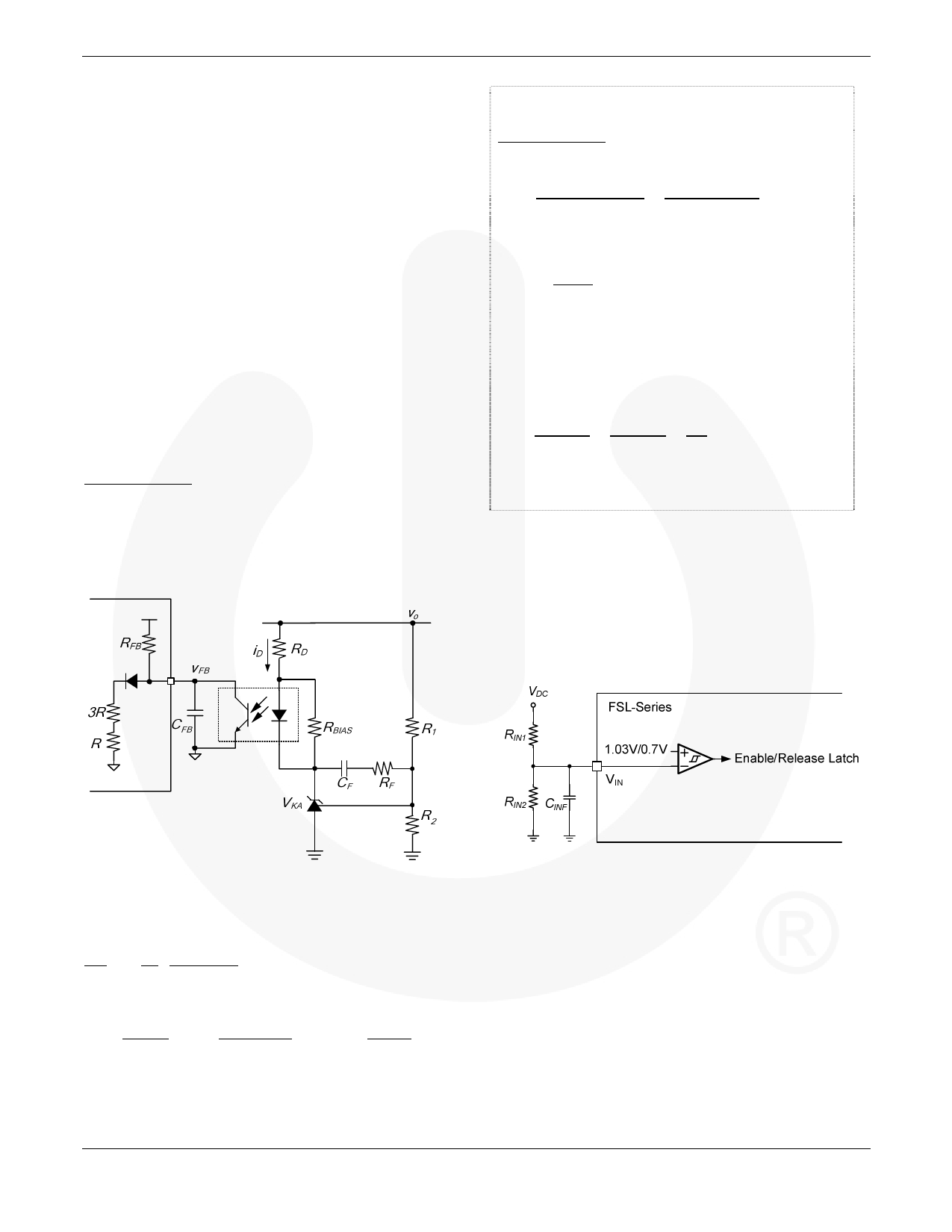
Figure 15 is a typical feedback circuit mainly consisting of a
shunt regulator and a photo-coupler. R1 and R2 form a
voltage divider for output voltage regulation. RF and CF are
for control-loop compensation. The maximum source
current of the FB pin is about 1mA. The phototransistor
must be capable of sinking this current to pull the FB level
down at no load. The value of RD, is determined by:
·
(23)
APPLICATION NOTE
(Design Example) Assuming CTR is 100%,
·
1 10
1 10
12 1.2 2.5
8.3 Ω
1 10
The minimum cathode current for KA431 is 1mA.
1.2 Ω.
1kΩ resistor is selected for RBIAS.
The voltage divider resistors R1 and R2 should be
designed to provide 2.5V to the reference pin of the
KA431.The relationship between R1 and R2 is given as:
2.5 ·
2.5 ·
2.5 12 2.5 3.8
38.2kΩ and 10kΩ resistor are selected for R1, R2.
where VOPD is the forward-voltage drop of the photodiode
(~1.2V); VKA is the minimum cathode-to-anode voltage of
KA431 (2.5V); and CTR is the current transfer rate of the
opto-coupler.
6V
[STEP-11] Design Input Voltage Sensing Circuit
Figure 16 shows a resistive voltage divider with low-pass
filter for line-voltage detection of the VIN pin. FSL-series
devices start and enable the latch function when the VIN
voltage reaches 1.03V. If latch protection is triggered, the
VIN voltage is used for release latch protection as the VIN
voltage drops below 0.7V. It is typical to use 100:1 voltage
divider for VIN level.
+
-
Figure 15. Feedback Circuit
The feedback compensation network transfer function of
Figure 15 is obtained as:
1⁄
·
1
⁄
(24)
where
1
,
1
(25)
Figure 16. Input Voltage Sensing
© 2010 Fairchild Semiconductor Corporation
Rev. 1.0.0 • 11/2/10
9
www.fairchildsemi.com
Share Link: 