FAN501MPX 데이터 시트보기 (PDF) - Fairchild Semiconductor
부품명
상세내역
일치하는 목록
FAN501MPX Datasheet PDF : 17 Pages
| |||
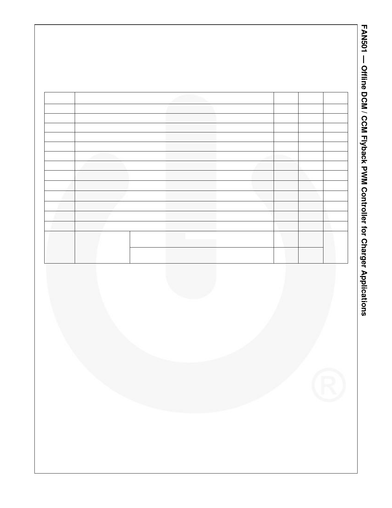
Absolute Maximum Ratings
Stresses exceeding the absolute maximum ratings may damage the device. The device may not function or be
operable above the recommended operating conditions and stressing the parts to these levels is not recommended.
In addition, extended exposure to stresses above the recommended operating conditions may affect device reliability.
The absolute maximum ratings are stress ratings only.
Symbol
Parameter
Min. Max. Unit
VHV
VVDD
VVS
VCS
VFB
VCOMP
VSD
PD
θJA
θJC
HV Pin Input Voltage
DC Supply Voltage
VS Pin Input Voltage
CS Pin Input Voltage
FB Pin Input Voltage
COMP Pin Input Voltage
SD Pin Input Voltage
Power Dissipation (TA=25C)
Thermal Resistance (Junction-to-Air)
Thermal Resistance (Junction-to-Case)
500
V
30
V
-0.3
6.0
V
-0.3
6.0
V
-0.3
6.0
V
-0.3
6.0
V
-0.3
6.0
V
850 mW
150 C/W
10 C/W
TJ Operating Junction Temperature
-40
+150
C
TSTG Storage Temperature Range
-40
+150
C
TL Lead Temperature (Wave soldering or IR, 10 Seconds)
+260
C
ESD
Electrostatic
Discharge
Capability(3)
Human Body Model, ANSI/ESDA/JEDEC JS-001-2012
(Except HV Pin)
Charged Device Model, JEDEC:JESD22_C101
(Except HV Pin)
5.0
kV
2.0
Notes:
1. All voltage values, except differential voltages, are given with respect to the GND pin.
2. Stresses beyond those listed under Absolute Maximum Ratings may cause permanent damage to the device.
3. ESD ratings including HV pin: HBM=3.0 kV, CDM=750 V.
© 2014 Fairchild Semiconductor Corporation
FAN501 • Rev. 1.0.0
4
www.fairchildsemi.com
Share Link: 