FAN501MPX 데이터 시트보기 (PDF) - Fairchild Semiconductor
부품명
상세내역
일치하는 목록
FAN501MPX Datasheet PDF : 17 Pages
| |||
The unified output current equation both for DCM and
CCM operation is obtained as:
IO=
NP
NS
∙IDS_Mid∙
tDIS
tS
=
NP
NS
∙
VCS_Mid
RCS
∙
tDIS
tS
(4)
VCS_Mid is obtained by sampling the current-sense
voltage at the middle of the MOSFET conduction time.
The diode current discharge time is obtained by
detecting the diode current zero-crossing instant. Since
the diode current cannot be sensed directly in the
primary side, Zero-Crossing Detection (ZCD) is
accomplished indirectly by monitoring the auxiliary
winding voltage in the primary side. When the diode
current reaches zero, the transformer winding voltage
begins to drop sharply. To detect the corner voltage, the
VS is sampled, called VSH, at 85% of diode current
discharge time (tDIS) of the previous switching cycle and
compared with the instantaneous VS voltage. When
instantaneous voltage of the VS pin drops below VSH by
more than 200 mV, the ZCD of diode current is
obtained, as shown in Figure 24.
The output current can be programmable by setting
current sensing resistor as:
RCS
1
IO
NP
NS
VCCR
KCC
(5)
where VCCR is the internal voltage for CC control and
KCC is the IC design parameter, 12 for the FAN501.
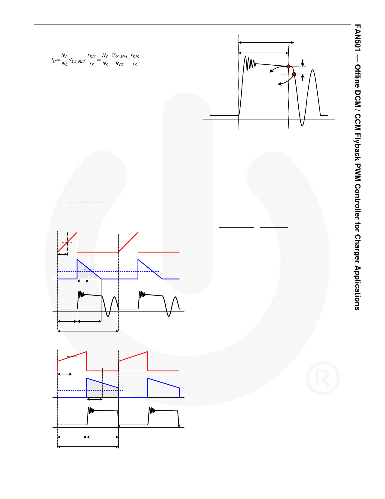
DCM Waveform
IDS-Mid
IDS
½ tON
ID
ID-Mid = NPS∙IDS-Mid
½ tDIS
IO = <ID>Ts
VS
tDIS(n)
0.85∙tDIS(n-1)
VS
VSH
ZCD
200mV
Figure 24. Operation Waveform for ZCD Function
Line Voltage Detection and its Utilization
The FAN501 indirectly senses line voltage using the
current flowing out of the VS pin while the MOSFET is
turned on, as illustrated in Figure 26 and Figure 27.
During the MOSFET turn-on period, auxiliary winding
voltage, VAux, reflects input bulk capacitor voltage, VBLK,
by the transformer coupling between primary and
auxiliary. During MOSFET conduction time, the line
voltage detector clamps the VS pin voltage ~0.5 V and
the current, IVS, flowing from the VS pin is expressed as:
IVS
NA
/ NP VBLK
RVS1
+
0.5
RVS1 / / RVS 2
(6)
Typically, the second term in Equation (6) can be
ignored because it is much smaller than the first term.
The current, IVS, is approximately proportional to the line
voltage, calculated as:
IVS
NA / NP
RVS1
VBLK
(7)
The IVS current, reflecting the line voltage information, is
used for dual switching frequency operation, CC control
correction weighting, and brownout protection; as
illustrated in Figure 26.
tON
Figure 22.
IDS-Mid
tDIS
tS
Waveforms of DCM Flyback Converter
CCM Waveform
IDS
½ tON
ID
ID-Mid = NPS∙IDS-Mid
IO = <ID>Ts
½ tDIS
VS
tON
Figure 23.
tDIS
tS
Waveforms of CCM Flyback Converter
© 2014 Fairchild Semiconductor Corporation
FAN501 • Rev. 1.0.0
Dual Switching Frequency
The FAN501 changes the switching frequency between
85 kHz and 140 kHz according to the line voltage. It is
typical to design the flyback converter to operate in
CCM for low line and DCM in high line. Therefore, the
peak transformer current decreases as the operation
mode changes from CCM to DCM, as shown in Figure
25(a), for single-frequency operation. The transformer is
not fully utilized at high line when a single switching
frequency is used. The peak transformer current can be
maintained almost constant when the flyback converter
operates at lower frequency at high line, as illustrated in
Figure 25(b). This allows full transformer utilization and
improves the efficiency by decreasing the switching
losses at high line.
When IVS is larger than IVS-H (750 µA), the switching
frequency is set at fOSC-L (85 kHz) in CV Mode. When IVS
is less than IVS-L (680 µA), the switching frequency is set
at fOSC-H (140 kHz) in CV Mode. For the universal line
range, the frequency change should occur between 132
~ 180 VAC to avoid the transition within the actual
www.fairchildsemi.com
11
Share Link: 