HIP2106IP 데이터 시트보기 (PDF) - Intersil
부품명
상세내역
일치하는 목록
HIP2106IP Datasheet PDF : 8 Pages
| |||
HIP2106
Electrical Specifications
PARAMETER
Peak Pulldown Current
VDD = VHB = 12V, VSS = VHS = 0V, No Load on LO or HO, Unless Otherwise Specified (Continued)
TJ = 25oC
TJ = -40oC
TO 125oC
SYMBOL
TEST CONDITIONS
MIN TYP MAX MIN MAX UNITS
IOLH
VHO = 12V
-
1
-
-
-
A
Switching Specifications VDD = VHB = 12V, VSS = VHS = 0V, No Load on LO or HO, Unless Otherwise Specified
TEST
TJ = 25oC
TTJ O= 1- 2450ooCC
PARAMETER
SYMBOL CONDITIONS MIN TYP MAX MIN MAX
UNITS
Lower Turn-Off Propagation Delay (LI Falling to LO Falling)
Upper Turn-Off Propagation Delay (HI Falling to HO Falling)
Lower Turn-On Propagation Delay (LI Rising to LO Rising)
Upper Turn-On Propagation Delay (HI Rising to HO Rising)
Delay Matching: Lower Turn-On and Upper Turn-Off
Delay Matching: Lower Turn-Off and Upper Turn-On
Either Output Rise/Fall Time
Either Output Rise/Fall Time (3V to 9V)
Either Output Rise Time Driving DMOS
Either Output Fall Time Driving DMOS
Minimum Input Pulse Width that Changes the Output
Bootstrap Diode Turn-On or Turn-Off Time
tLPHL
tHPHL
tLPLH
tHPLH
tMON
tMOFF
tRC, tFC
tR, tF
tRD
tFD
tPW
tBS
CL = 1000pF
CL = 0.1µF
CL = IRFR120
CL = IRFR120
-
40 70
-
90
ns
-
40 70
-
90
ns
-
40 70
-
90
ns
-
40 70
-
90
ns
-
4
16
-
20
ns
-
4
16
-
20
ns
- 20 -
-
-
ns
- 1.0 1.2 - 1.6 us
- 40 -
-
-
ns
- 20 -
-
-
ns
-
-
-
- 100 ns
- 20 -
-
-
ns
Pin Descriptions
PIN
NUMBER
1
2
3
4
5
6
7
8
SYMBOL
VDD
HB
HO
HS
HI
LI
VSS
LO
DESCRIPTION
Positive Supply to lower gate drivers. De-couple this pin to VSS (Pin 7). Bootstrap diode connected to HB (pin 2).
High-Side Bootstrap supply. External bootstrap capacitor is required. Connect positive side of bootstrap capacitor to
this pin. Bootstrap diode is on-chip.
High-Side Output. Connect to gate of High-Side power MOSFET.
High-Side Source connection. Connect to source of High-Side power MOSFET. Connect negative side of bootstrap
capacitor to this pin.
High-Side input.
Low-Side input.
Chip negative supply, generally will be ground.
Low-Side Output. Connect to gate of Low-Side power MOSFET.
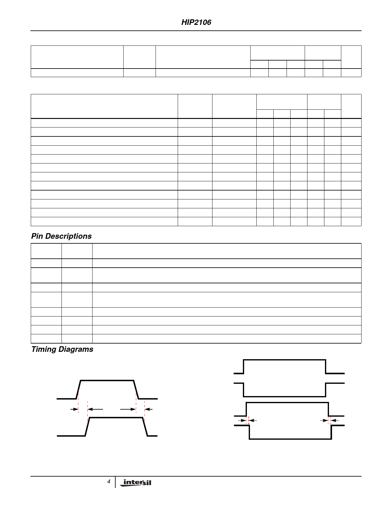
Timing Diagrams
LI
HI,
LI
tHPLH ,
tLPLH
tHPHL,
tLPHL
HO,
LO
FIGURE 3.
HI
LO
tMON
HO
tMOFF
FIGURE 4.
4
Share Link: 