HIP2106IP 데이터 시트보기 (PDF) - Intersil
부품명
상세내역
일치하는 목록
HIP2106IP Datasheet PDF : 8 Pages
| |||
HIP2106
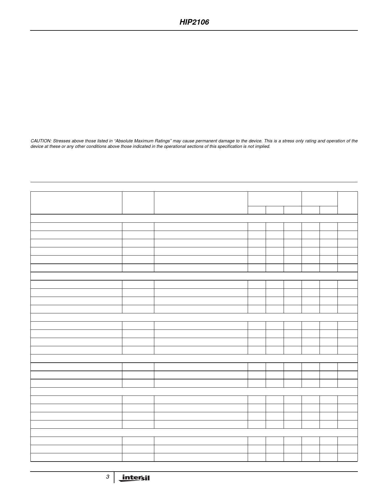
Absolute Maximum Ratings
Supply Voltage, VDD, VHB-VHS . . . . . . . . . . . . . . . . . . . -0.3V to 18V
LI and HI Voltages . . . . . . . . . . . . . . . . . . . . . . . . .-3V to VDD +0.3V
Voltage on LO . . . . . . . . . . . . . . . . . . . . . . . . . . -0.3V to VDD +0.3V
Voltage on HO . . . . . . . . . . . . . . . . . . . . . . VHS -0.3V to VHB +0.3V
Voltage on HS (Continuous) . . . . . . . . . . . . . . . . . . . . . -1V to 110V
Voltage on HB . . . . . . . . . . . . . . . . . . . . . . . . . . . . . . . . . . . . +118V
Average Current in VDD to HB Diode. . . . . . . . . . . . . . . . . . . 100mA
ESD Classification . . . . . . . . . . . . . . . . . . . . . . . . . . . . Class 1 (1kV)
Recommended Operating Conditions
Supply Voltage, VDD . . . . . . . . . . . . . . . . . . . . . . . . . +9V to +16.5V
Voltage on HS . . . . . . . . . . . . . . . . . . . . . . . . . . . . . . . . -1V to 100V
Thermal Information
Thermal Resistance (Typical, Note 1)
θJA (oC/W)
SOIC Package . . . . . . . . . . . . . . . . . . . . . . . . . . . . .
160
PDIP Package . . . . . . . . . . . . . . . . . . . . . . . . . . . . .
100
HS Slew Rate . . . . . . . . . . . . . . . . . . . . . . . . . . . . . . . . . . . 10V/ns
Maximum Power Dissipation at 25oC in Free Air . . . . . . . . . .780mW
Maximum Storage Temperature Range . . . . . . . . . . -65oC to 150oC
Maximum Junction Temperature Range . . . . . . . . . -55oC to 150oC
Maximum Lead Temperature (Soldering 10s) . . . . . . . . . . . . .300oC
(Lead Tips Only)
Voltage on HS . . . . . . . . . . . . . . . (Repetitive Transient) -5V to 105V
Voltage on HB. . . VHS +8V to VHS +16.5V and VDD -1V to VDD +100V
CAUTION: Stresses above those listed in “Absolute Maximum Ratings” may cause permanent damage to the device. This is a stress only rating and operation of the
device at these or any other conditions above those indicated in the operational sections of this specification is not implied.
NOTES:
1. θJA is measured with the component mounted on an evaluation PC board in free air.
2. All Voltages Relative to Pin 4, VSS Unless Otherwise Specified.
Electrical Specifications
PARAMETER
VDD = VHB = 12V, VSS = VHS = 0V, No Load on LO or HO, Unless Otherwise Specified
TJ = 25oC
TTJO=1-2450ooCC
SYMBOL
TEST CONDITIONS
MIN TYP MAX MIN MAX
SUPPLY CURRENTS
VDD Quiescent Current
VDD Operating Current
Total HB Quiescent Current
Total HB Operating Current
HB to VSS Current, Quiescent
HB to VSS Current, Operating
INPUT PINS
IDD
IDDO
IHB
IHBO
IHBS
IHBSO
LI = HI = 0V
f = 500kHz
LI = HI = 0V
f = 500kHz
VHS = VHB = 116.5V
f = 500kHz
-
0.1 0.15 -
0.2
-
1.5 2.5
-
3
-
0.1 0.15 -
0.2
-
1.5 2.5
-
3
- 0.05 1
-
10
-
0.7
-
-
-
Low Level Input Voltage Threshold
High Level Input Voltage Threshold
Input Voltage Hysteresis
Input Pulldown Resistance
UNDER VOLTAGE PROTECTION
VIL
VIH
VIHYS
RI
4
5.4
-
3
-
-
5.8
8
-
9
-
0.4
-
-
-
- 200 - 100 500
VDD Rising Threshold
VDD Threshold Hysteresis
HB Rising Threshold
HB Threshold Hysteresis
BOOT STRAP DIODE
VDDR
VDDH
VHBR
VHBH
7
7.3
8
6.5 8.5
-
0.5
-
-
-
6.5 6.9 7.5 6
8
-
0.4
-
-
-
Low-Current Forward Voltage
High-Current Forward Voltage
Dynamic Resistance
LO GATE DRIVER
VDL
VDH
RD
IVDD-HB = 100µA
IVDD-HB = 100mA
IVDD-HB = 100mA
- 0.45 0.55 -
0.7
-
0.7 0.8
-
1
-
0.8
1
-
1.5
Low Level Output Voltage
High Level Output Voltage
Peak Pullup Current
Peak Pulldown Current
HO GATE DRIVER
VOLL
VOHL
IOHL
IOLL
ILO = 100mA
ILO = -100mA, VOHL = VDD-VLO
VLO = 0V
VLO = 12V
- 0.25 0.3
-
0.4
- 0.25 0.3
-
0.4
-
1
-
-
-
-
1
-
-
-
Low Level Output Voltage
High Level Output Voltage
Peak Pullup Current
VOLH
VOHH
IOHH
IHO = 100mA
IHO = -100mA, VOHH = VHB-VHO
VHO = 0V
- 0.25 0.3
-
0.4
- 0.25 0.3
-
0.4
-
1
-
-
-
UNITS
mA
mA
mA
mA
µA
mA
V
V
V
kΩ
V
V
V
V
V
V
Ω
V
V
A
A
V
V
A
3
Share Link: 