CS8164 데이터 시트보기 (PDF) - Cherry semiconductor
부품명
상세내역
일치하는 목록
CS8164 Datasheet PDF : 8 Pages
| |||
Application Notes: continued
Step 3: Increase the ESR of the capacitor from zero using
the decade box and vary the load current until oscillations
appear. Record the values of load current and ESR that
cause the greatest oscillation. This represents the worst
case load conditions for the output at low temperature.
Step 4: Maintain the worst case load conditions set in step
3 and vary the input voltage until the oscillations increase.
This point represents the worst case input voltage condi-
tions.
Step 5: If the capacitor is adequate, repeat steps 3 and 4
with the next smaller valued capacitor. A smaller capacitor
will usually cost less and occupy less board space. If the
output oscillates within the range of expected operating
conditions, repeat steps 3 and 4 with the next larger stan-
dard capacitor value.
Step 6: Test the load transient response by switching in
various loads at several frequencies to simulate its real
working environment. Vary the ESR to reduce ringing.
Step 7: Remove the unit from the environmental chamber
and heat the IC with a heat gun. Vary the load current as
instructed in step 5 to test for any oscillations.
Once the minimum capacitor value with the maximum
ESR is found for each output, a safety factor should be
added to allow for the tolerance of the capacitor and any
variations in regulator performance. Most good quality
aluminum electrolytic capacitors have a tolerance of +/-
20% so the minimum value found should be increased by
at least 50% to allow for this tolerance plus the variation
which will occur at low temperatures. The ESR of the
capacitors should be less than 50% of the maximum allow-
able ESR found in step 3 above.
Repeat steps 1 through 7 with the capacitor on the other
output, C3.
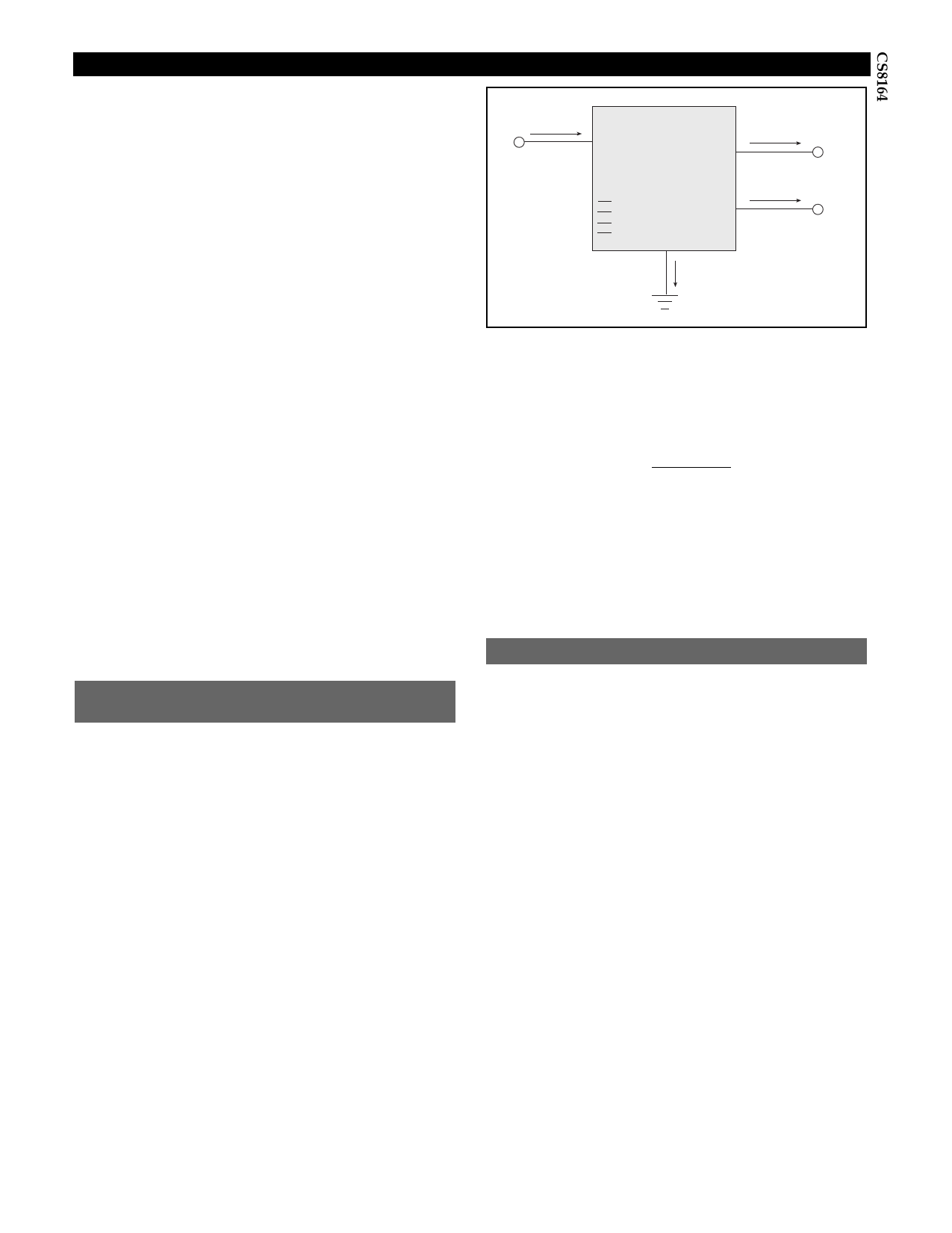
IIN
VIN
Smart
Regulator
}Control
Features
IQ
IOUT1
IOUT2
VOUT1
VOUT2
Figure 1: Dual output regulator with key performance parameters
labeled.
Once the value of PD(max) is known, the maximum permis-
sible value of RQJA can be calculated:
RQJA =
150¡C - TA
PD
(2)
The value of RQJA can then be compared with those in the
package section of the data sheet. Those packages with
RQJA's less than the calculated value in equation 2 will keep
the die temperature below 150¡C.
In some cases, none of the packages will be sufficient to
dissipate the heat generated by the IC, and an external
heatsink will be required.
Heat Sinks
Calculating Power Dissipation
in a Dual Output Linear Regulator
The maximum power dissipation for a dual output regula-
tor (Figure 1) is:
PD(max) = {VIN(max) - VOUT1(min)}IOUT1(max)+
{VIN(max) - VOUT2(min)}IOUT2(max)+VIN(max)IQ
(1)
where:
VIN(max) is the maximum input voltage,
VOUT1(min) is the minimum output voltage from VOUT1,
VOUT2(min) is the minimum output voltage from VOUT2,
IOUT1(max) is the maximum output current for the applica-
tion,
IOUT2(max) is the maximum output current for the applica-
tion, and
IQ is the quiescent current the regulator consumes at
IOUT(max).
A heat sink effectively increases the surface area of the
package to improve the flow of heat away from the IC and
into the surrounding air.
Each material in the heat flow path between the IC and the
outside environment will have a thermal resistance. Like
series electrical resistances, these resistances are summed
to determine the value of RQJA:
RQJA = RQJC + RQCS + RQSA
(3)
where:
RQJC = the junction-to-case thermal resistance,
RQCS = the case-to-heatsink thermal resistance, and
RQSA = the heatsink-to-ambient thermal resistance.
RQJC appears in the package section of the data sheet. Like
RQJA, it too is a function of package type. RQCS and RQSA
are functions of the package type, heatsink and the inter-
face between them. These values appear in heat sink data
sheets of heat sink manufacturers.
7
Share Link: 