IRF1607 데이터 시트보기 (PDF) - International Rectifier
부품명
상세내역
일치하는 목록
IRF1607 Datasheet PDF : 9 Pages
| |||
IRF1607
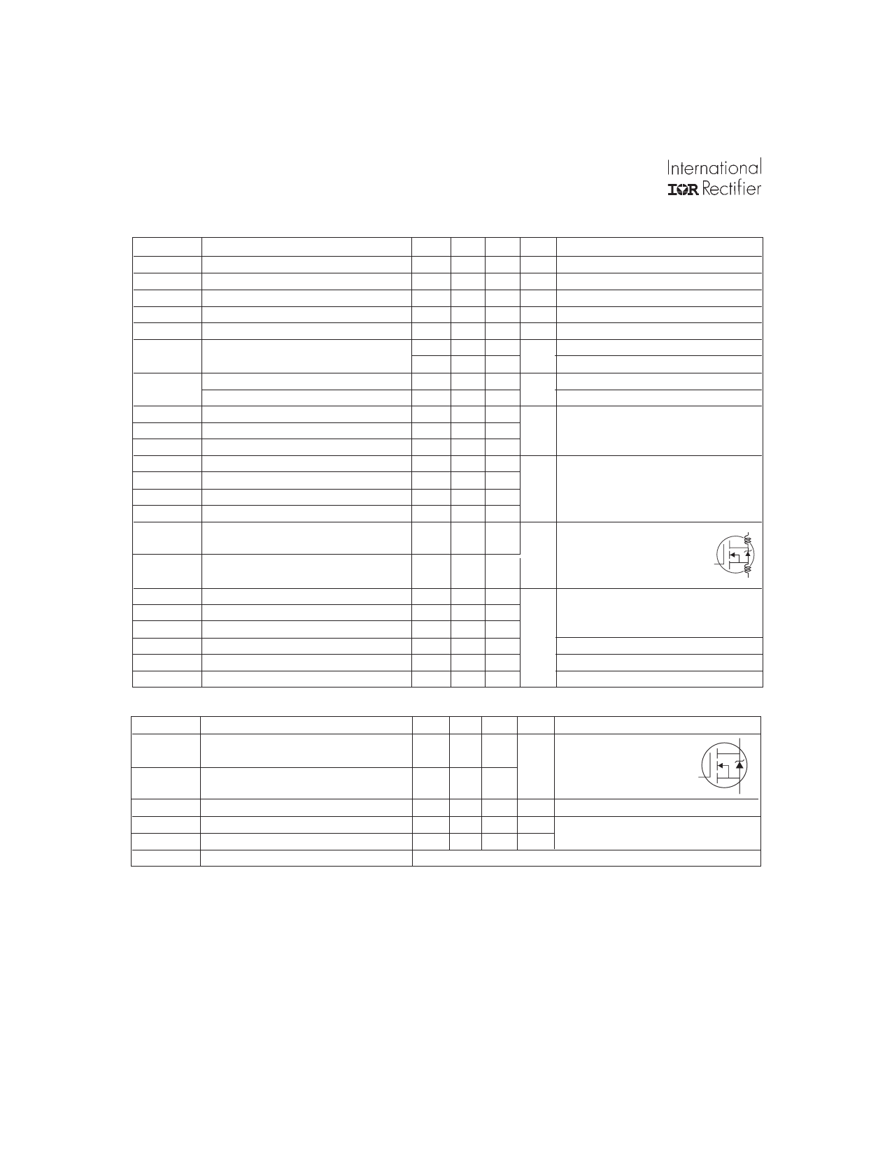
Electrical Characteristics @ TJ = 25°C (unless otherwise specified)
Parameter
V(BR)DSS
∆V(BR)DSS/∆TJ
RDS(on)
VGS(th)
gfs
Drain-to-Source Breakdown Voltage
Breakdown Voltage Temp. Coefficient
Static Drain-to-Source On-Resistance
Gate Threshold Voltage
Forward Transconductance
IDSS
Drain-to-Source Leakage Current
IGSS
Qg
Qgs
Qgd
td(on)
tr
td(off)
tf
Gate-to-Source Forward Leakage
Gate-to-Source Reverse Leakage
Total Gate Charge
Gate-to-Source Charge
Gate-to-Drain ("Miller") Charge
Turn-On Delay Time
Rise Time
Turn-Off Delay Time
Fall Time
LD
Internal Drain Inductance
LS
Ciss
Coss
Crss
Coss
Coss
Coss eff.
Internal Source Inductance
Input Capacitance
Output Capacitance
Reverse Transfer Capacitance
Output Capacitance
Output Capacitance
Effective Output Capacitance
Min. Typ. Max. Units
Conditions
75 ––– ––– V VGS = 0V, ID = 250µA
––– 0.086 ––– V/°C Reference to 25°C, ID = 1mA
––– 0.00580.0075 Ω VGS = 10V, ID = 85A
2.0 ––– 4.0
79 ––– –––
V VDS = 10V, ID = 250µA
S VDS = 25V, ID = 85A
––– ––– 20
––– ––– 250
µA VDS = 75V, VGS = 0V
VDS = 60V, VGS = 0V, TJ = 150°C
––– ––– 200 nA VGS = 20V
––– ––– -200
VGS = -20V
––– 210 320
ID = 85A
––– 45 68 nC VDS = 60V
––– 73 110
––– 22 –––
VGS = 10V
VDD = 38V
––– 130 ––– ns ID = 85A
––– 84 –––
RG = 1.8Ω
––– 86 –––
VGS = 10V
Between lead,
D
––– 4.5 –––
6mm (0.25in.)
nH
from package
G
––– 7.5 –––
and center of die contact
S
––– 7750 –––
VGS = 0V
––– 1230 ––– pF VDS = 25V
––– 310 –––
ƒ = 1.0MHz, See Fig. 5
––– 5770 –––
––– 790 –––
VGS = 0V, VDS = 1.0V, ƒ = 1.0MHz
VGS = 0V, VDS = 60V, ƒ = 1.0MHz
––– 1420 –––
VGS = 0V, VDS = 0V to 60V
Source-Drain Ratings and Characteristics
Parameter
Min. Typ. Max. Units
Conditions
IS
Continuous Source Current
(Body Diode)
ISM
Pulsed Source Current
(Body Diode)
MOSFET symbol
D
––– ––– 142
A
showing the
integral reverse
G
––– ––– 570
p-n junction diode.
S
VSD
Diode Forward Voltage
trr
Reverse Recovery Time
Qrr
Reverse RecoveryCharge
ton
Forward Turn-On Time
––– ––– 1.3 V TJ = 25°C, IS = 85A, VGS = 0V
––– 130 200 ns TJ = 25°C, IF = 85A
––– 690 1040 nC di/dt = 100A/µs
Intrinsic turn-on time is negligible (turn-on is dominated by LS+LD)
Notes:
Repetitive rating; pulse width limited by
Coss eff. is a fixed capacitance that gives the same charging time
max. junction temperature. (See fig. 11).
Starting TJ = 25°C, L = 0.21mH
RG = 25Ω, IAS = 85A, VGS=10V (See Figure 12).
ISD ≤ 85A, di/dt ≤ 310A/µs, VDD ≤ V(BR)DSS,
TJ ≤ 175°C
as Coss while VDS is rising from 0 to 80% VDSS .
Calculated continuous current based on maximum allowable
junction temperature. Package limitation current is 75A.
Limited by TJmax , see Fig.12a, 12b, 15, 16 for typical repetitive
Pulse width ≤ 400µs; duty cycle ≤ 2%.
avalanche performance.
2
www.irf.com
Share Link: 