NCP1560 데이터 시트보기 (PDF) - ON Semiconductor
부품명
상세내역
일치하는 목록
NCP1560 Datasheet PDF : 20 Pages
| |||
NCP1560
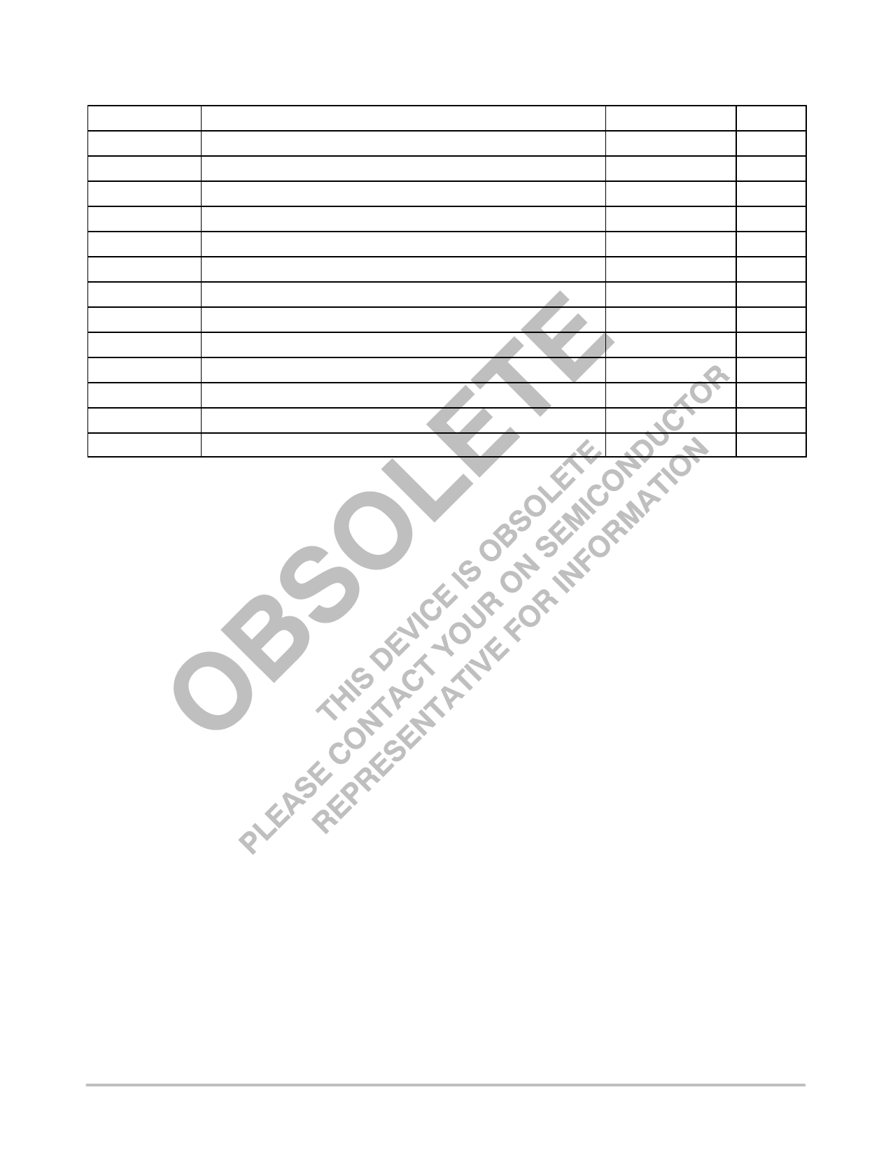
MAXIMUM RATINGS
Symbol
Rating
Value
Unit
Vin
Input Line Voltage
−0.3 to 150
V
VAUX
Auxiliary Supply Voltage
−0.3 to 16
V
IAUX
Auxiliary Supply Input Current
35
mA
VOUT
OUT1 and OUT2 Voltage
−0.3 to (VAUX + 0.3 V)
V
IOUT
OUT1 and OUT2 Output Current
10
mA
VREF
5.0 V Reference Voltage
−0.3 to 6.0
V
IREF
5.0 V Reference Output Current
6.0
mA
VIO
All Other Inputs/Outputs Voltage
−0.3 to VREF
V
IIO
All Other Inputs/Outputs Current
10
mA
TJ
Operating Junction Temperature
−40 to 125
°C
Tstg
Storage Temperature Range
−55 to 150
°C
PD
Power Dissipation at TA = 25°C
0.77
W
RqJA
Thermal Resistance, Junction−to−Ambient
130
°C/W
Stresses exceeding Maximum Ratings may damage the device. Maximum Ratings are stress ratings only. Functional operation above the
Recommended Operating Conditions is not implied. Extended exposure to stresses above the Recommended Operating Conditions may affect
device reliability.
1. This device series contains ESD protection and exceeds the following tests:
Pin 1 is the HV startup of the device and is rated to the max rating of the part, or 150 V.
Machine Model Method 150 V.
Pins 2−16: Human Body Model 4000 V per MIL−STD−883, Method 3015.
Machine Model Method 200 V.
http://onsemi.com
5
Share Link: 