7641 데이터 시트보기 (PDF) - Mitsumi
부품명
상세내역
일치하는 목록
7641 Datasheet PDF : 149 Pages
| |||
PRELIMINARY NSocothimcaene:gpTeah.riasmisetnrioct laimfiintsalasrepescuibfijceacttioton.
MITSUBISHI MICROCOMPUTERS
7641 Group
SINGLE-CHIP 8-BIT CMOS MICROCOMPUTER
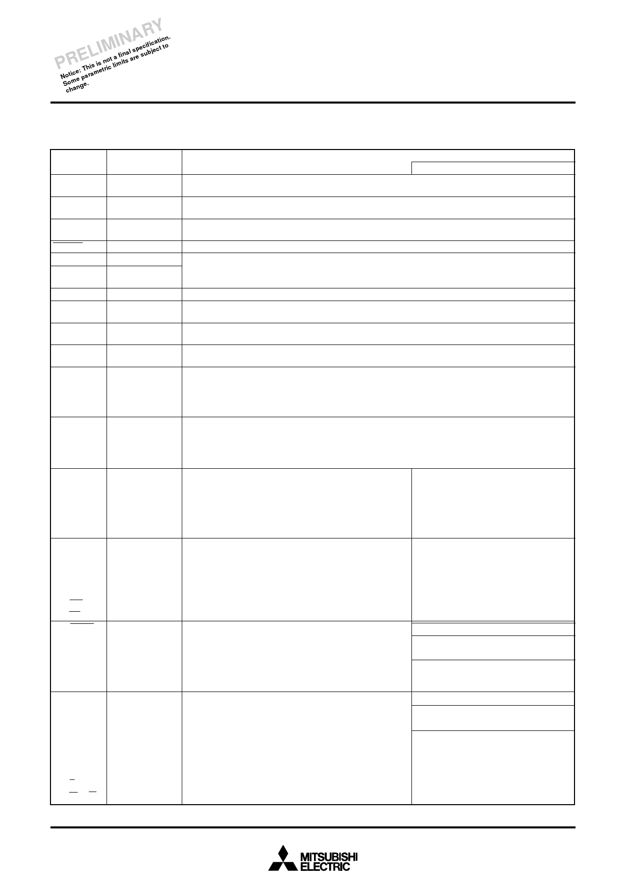
PIN DESCRIPTION
Table 1 Pin description (1)
Pin
Name
VCC, VSS
Power source
CNVss/VPP CNVss
AVss/AVcc
RESET
XIN
XOUT
Analog power
supply
Reset input
Clock input
Clock output
LPF
Ext. Cap.
USB D+
LPF
3.3 V line power
supply
USB D+
USB D-
USB D-
P00/AB0–
P07/AB7
I/O port P0
P10/AB8–
P17/AB15
I/O port P1
P20/DB0–
P27/DB7
I/O port P2
P30/RDY,
I/O port P3
P31, P32,
(See Remarks.)
P33/DMAOUT,
P34/φ OUT,
P35/SYNCOUT,
P36/WR,
P37/RD
P40/EDMA, I/O port P4
P41/INT0,
P42/INT1,
P43/CNTR0,
P44/CNTR1
P50/XCIN,
P51/TOUT/
XCOUT,
P52/OBF0,
P53/IBF0,
P54/S0,
P55/A0,
P56/R(E),
P57/W(R/W)
I/O port P5
Function
Function except a port function
• Apply 4.15 V – 5.25 V for 5 V version or 3.00 V – 3.60 V for 3 V version to the Vcc pin. Apply 0 V to the
Vss pin.
• This controls the MCU operating mode. Connect this pin to Vss. If connecting this pin to Vcc, the
internal ROM is inhibited. In the flash memory version this pin functions as a VPP power supply input pin.
• These pins are the power supply inputs for analog circuitry.
• Reset input pin for active “L.”
• Connect a ceramic resonator or a quartz-crystal oscillator between the XIN and XOUT pins to set the
oscillation frequency.
• If an external clock is used, connect the clock source to the XIN pin and leave the XOUT pin open.
• Loop filter for the frequency synthesizer.
• Power supply input pin for 3.3 V USB line driver.
• USB D+ voltage signal port. Connect a 27 to 33 Ω (recommended) resistor in series.
• USB D- voltage signal port. Connect a 27 to 33 Ω (recommended) resistor in series.
• 8-bit I/O port.
• CMOS compatible input level.
• CMOS 3-state output structure.
• I/O direction register allows each pin to be individually programmed as either input or output.
• When connecting an external memory, these function as the address bus.
• 8-bit I/O port.
• CMOS compatible input level.
• CMOS 3-state output structure.
• I/O direction register allows each pin to be individually programmed as either input or output.
• When connecting an external memory, these function as the address bus.
• 8-bit I/O port.
• CMOS compatible input level or VIHL input level.
• CMOS 3-state output structure.
• I/O direction register allows each pin to be individually
programmed as either input or output.
• When connecting an external memory, these function as
the data bus.
• Key-on wake-up interrupt input pin
• 8-bit I/O port.
• CMOS compatible input level.
• CMOS 3-state output structure.
• I/O direction register allows each pin to be individually
programmed as either input or output.
• When connecting an external memory, these function as
the control bus.
• External memory control pin
• 8-bit I/O port.
• CMOS compatible input level.
• CMOS 3-state output structure.
• I/O direction register allows each pin to be individually
programmed as either input or output.
• When connecting an external memory, these function as
the control bus.
• 8-bit I/O port.
• CMOS compatible input level.
• CMOS 3-state output structure.
• I/O direction register allows each pin to be individually
programmed as either input or output.
• When enabling the Master CPU bus interface function,
CMOS or TTL input level can be selected as an input.
• External memory control pin
• External interrupt pin
• Timer X, Timer Y pin
• Sub-clock generating input pin
• Timers 1, 2 pulse output pins
• Sub-clock generating output pin
• Master CPU bus interface pin
4
Share Link: 