HT761X 데이터 시트보기 (PDF) - Holtek Semiconductor
부품명
상세내역
일치하는 목록
HT761X Datasheet PDF : 12 Pages
| |||
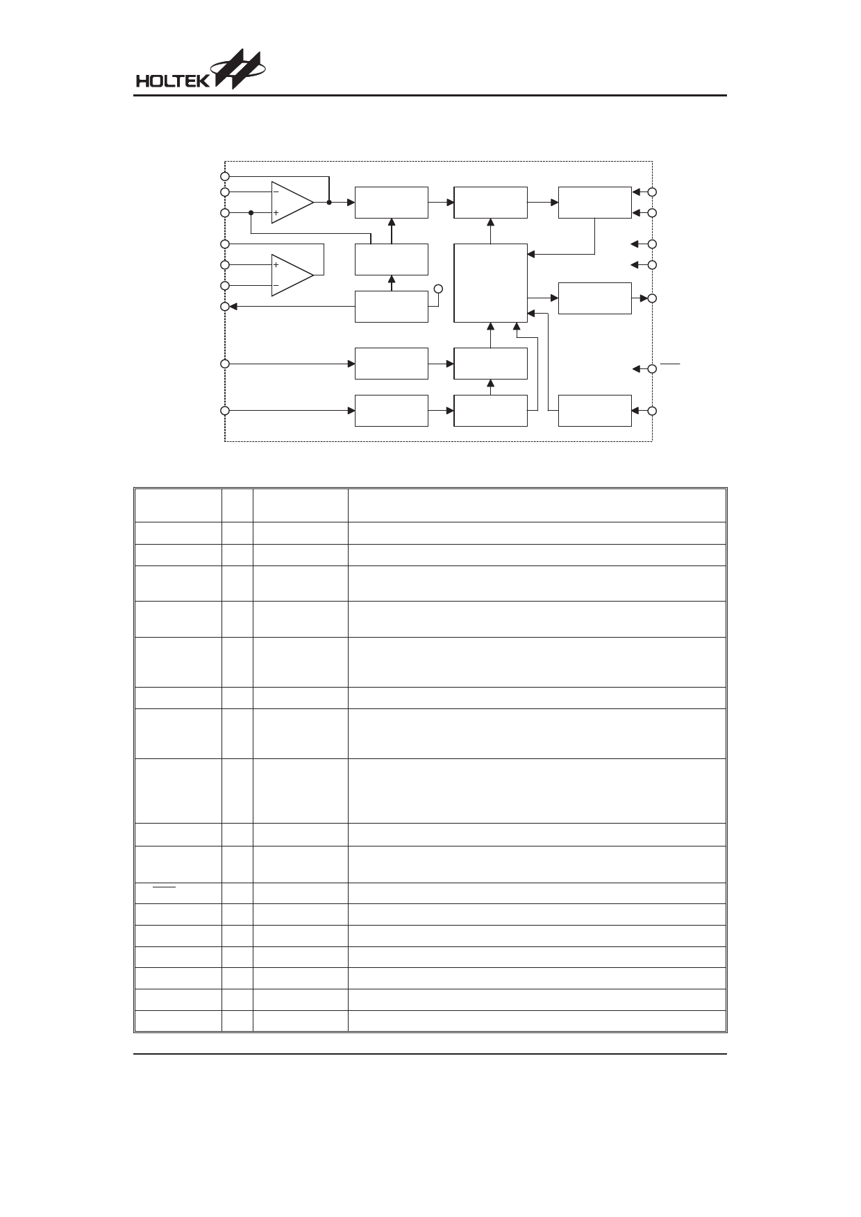
Block Diagram
O P 2O
O P 2N
O P 2P
O P 1O
O P 1P
O P 1N
VEE
O SCD
O SCS
HT761X
C o m p a ra to r
L a tc h C ir c u it
V o lta g e
D iv id e r
V DD
R e g u la to r
C o n tro l
C ir c u it
M ode & C D S
C ir c u it
O u tp u t C ir c u it
M ODE
CDS
VSS
VDD
R E LA Y
(T R IA C )
D e la y
O s c illa to r
S y s te m
O s c illa to r
D e la y C ir c u it
C o u n te r
C ir c u it
RST
Z e ro C ro s s
D ebounce
ZC
Pin Description
Pin Name I/O
VSS
¾
RELAY
O
TRIAC
O
OSCD
I/O
OSCS
I/O
ZC
I
CDS
I
MODE
I
VDD
¾
VEE
O
RST
I
OP1P
I
OP1N
I
OP1O
O
OP2P
I
OP2N
I
OP2O
O
Internal
Connection
¾
CMOS
CMOS
PMOS IN
NMOS OUT
PMOS IN
NMOS OUT
CMOS
CMOS
CMOS
¾
NMOS
Pull-High
PMOS
PMOS
NMOS
PMOS
PMOS
NMOS
Description
Negative power supply, ground
RELAY drive output through an external NPN transistor, active high.
TRIAC drive output
The output is a pulse output when active.
Output timing oscillator I/O
It is connected to an external RC to adjust output duration.
System oscillator I/O
OSCS is connected to an external RC to set the system frequency. The
system frequency is at 16kHz for normal application.
Input for AC zero crossing detection
CDS is connected to a CDS voltage divider for daytime/night
auto-detection. Low input to this pin can disable the PIR input. CDS a
Schmitt Trigger input with 5-second input debounce time.
Operating mode selection input:
VDD: Output is always ON
VSS: Output is always OFF
Open: Auto detection
Positive power supply
Regulated voltage output
The output voltage is -4V with respect to VDD.
Chip reset input, active low
Noninverting input of OP1
Inverting input of OP1
Output of OP1
Noninverting input of OP2
Inverting input of OP2
Output of OP2
Rev. 1.30
2
October 12, 2009
Share Link: 