HEF4050BT(2016) 데이터 시트보기 (PDF) - NXP Semiconductors.
부품명
상세내역
일치하는 목록
HEF4050BT Datasheet PDF : 12 Pages
| |||
Nexperia
HEF4050B
Hex non-inverting buffers
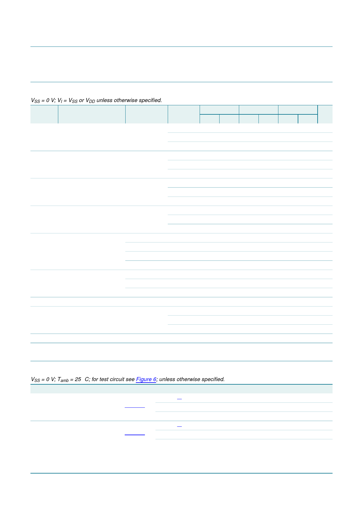
8. Limiting values
Table 4. Limiting values
In accordance with the Absolute Maximum Rating System (IEC 60134).
Symbol Parameter
Conditions
Min
VDD
supply voltage
IIK
input clamping current
VI < 0.5 V
VI
input voltage
IOK
output clamping current
VO < 0.5 V or VO > VDD + 0.5 V
0.5
10
0.5
-
II/O
input/output current
-
IDD
Tstg
Tamb
Ptot
supply current
storage temperature
ambient temperature
total power dissipation
Tamb 40 C to +85 C
SO16 package
-
65
40
[1]
-
P
power dissipation
per output
-
[1] For SO16 package: Ptot derates linearly with 8 mW/K above 70 C.
9. Recommended operating conditions
Max Unit
+18
V
-
mA
+18
V
10
mA
10
mA
50
mA
+150 C
+85
C
500
mW
100
mW
Table 5.
Symbol
VDD
VI
Tamb
t/V
Recommended operating conditions
Parameter
Conditions
supply voltage
input voltage
ambient temperature
in free air
input transition rise and fall rate
VDD = 5 V
VDD = 10 V
VDD = 15 V
10. Static characteristics
Min
Max Unit
3
15
V
0
15 V
40
+85 C
-
3.75 s/V
-
0.5 s/V
-
0.08 s/V
Table 6. Static characteristics
VSS = 0 V; VI = VSS or VDD unless otherwise specified.
Symbol Parameter
Conditions
VDD
VIH
HIGH-level input voltage IO < 1 A
5V
10 V
15 V
VIL
LOW-level input voltage IO < 1 A
5V
10 V
15 V
Tamb = 40 C Tamb = 25 C
Min Max Min Max
3.5
-
3.5
-
7.0
-
7.0
-
11.0 - 11.0 -
-
1.5
-
1.5
-
3.0
-
3.0
-
4.0
-
4.0
Tamb = 85 C Unit
Min Max
3.5
-V
7.0
-V
11.0 - V
-
1.5 V
-
3.0 V
-
4.0 V
HEF4050B
Product data sheet
All information provided in this document is subject to legal disclaimers.
Rev. 10 — 23 June 2016
© Nexperia B.V. 2017. All rights reserved
4 of 12
Share Link: 