PI74FCT3244R 데이터 시트보기 (PDF) - Pericom Semiconductor
부품명
상세내역
일치하는 목록
PI74FCT3244R Datasheet PDF : 4 Pages
| |||
PI74FCT3244
11223344556677889900112233445566778899001122334455667788990011221122334455667788990011223344556677889900112233445566778899001122112233445566778899001122334455667788990011223344556637788.39900V112211822-3344B5566I77T889900B1122U3344F5566F7788E9900R1122/33L4455I66N778899E001122D1122R3344I55V667788E9900R1122
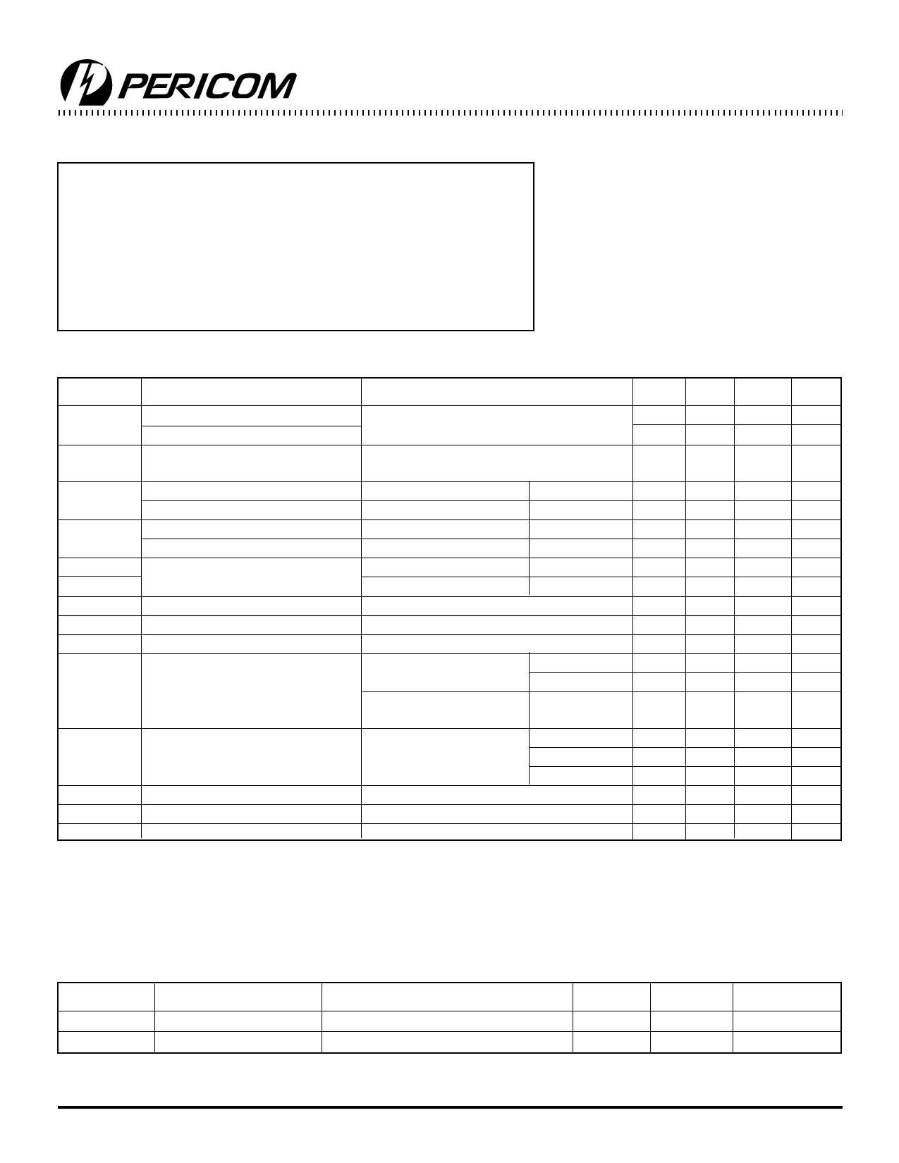
Maximum Ratings
(Above which the useful life may be impaired. For user guidelines, not tested.)
Storage Temperature .............................................................. –65°C to +150°C
Ambient Temperature with Power Applied ............................. –40°C to +85°C
Supply Voltage to Ground Potential (Inputs & Vcc Only) ....... –0.5V to +7.0V
Supply Voltage to Ground Potential (Outputs & D/O Only) ... –0.5V to +7.0V
DC Input Voltage ..................................................................... –0.5V to +7.0V
DC Output Current ............................................................................... 120 mA
Power Dissipation ..................................................................................... 1.0W
Note:
Stresses greater than those listed under MAXIMUM
RATINGS may cause permanent damage to the
device. This is a stress rating only and functional
operation of the device at these or any other condi-
tions above those indicated in the operational sec-
tions of this specification is not implied. Exposure to
absolute maximum rating conditions for extended
periods may affect reliability.
DC Electrical Characteristics (Over the Operating Range, TA = –40°C to +85°C, VCC = 2.7V to 3.6V)
Parameters
Description
Test Conditions(1)
Min. Typ.(2) Max. Units
VIH
VIL
IIH
IIL
IOZH
IOZL
VIK
IODH
IODL
VOH
VOL
IOS
IOFF
VH
Input HIGH Voltage (Input pins) Guaranteed Logic HIGH Level
2.2 — 5.5 V
Input HIGH Voltage (I/O pins)
2.0 — 5.5 V
Input LOW Voltage
Guaranteed Logic LOW Level
–0.5 — 0.8 V
(Input and I/O pins)
Input HIGH Current (Input pins) VCC = Max.
VIN = 5.5V
— — ±1 µA
Input HIGH Current (I/O pins) VCC = Max.
VIN = VCC
— — ±1 µA
Input LOW Current (Input pins) VCC = Max.
VIN = GND
— — ±1 µA
Input LOW Current (I/O pins)
VCC = Max.
VIN = GND
— — ±1 µA
High Impedance Output Current VCC = Max.
VOUT = 5.5V —
—
±1
µA
(3-State Output pins)
VCC = Max.
VOUT = GND —
—
±1
µA
Clamp Diode Voltage
VCC = Min., IIN = –18mA
— –0.7 –1.2 V
Output HIGH Current
VCC = 3.3V, VIN = VIH or VIL, VO = 1.5V(3) –36 –60 –110 mA
Output LOW Current
VCC = 3.3V, VIN = VIH or VIL, VO = 1.5V(3) 50
90 200 mA
Output HIGH Voltage
VCC = Min.
IOH = –0.1mA Vcc-0.2 —
—
V
VIN = VIH or VIL
IOH = –3mA
2.4 3.0 —
V
VCC = 3.0V,
IOH = –8mA 2.4(5) 3.0
—
V
VIN = VIH or VIL
IOH = –24mA 2.0
—
—
Output LOW Voltage
VCC = Min.
IOL = 0.1mA
—
—
0.2
V
VIN = VIH or VIL
IOL = 16mA
— 0.2 0.4 V
Short Circuit Current(4)
IOL = 24mA
VCC = Max.(3), VOUT = GND
— 0.3 0.5 V
–60 –85 –240 mA
Power Down Disable
VCC = 0V, VIN or VOUT ≤ 4.5V
— — ±100 µA
Input Hysteresis
— 150 — mV
Notes:
1. For Max. or Min. conditions, use appropriate value specified under Electrical Characteristics for the applicable device type.
2. Typical values are at Vcc = 3.3V, +25°C ambient and maximum loading.
3. Not more than one output should be shorted at one time. Duration of the test should not exceed one second.
4. This parameter is guaranteed but not tested.
5. VOH = VCC – 0.6V at rated current.
Capacitance (TA = 25°C, f = 1 MHz)
Parameters(1) Description
Test Conditions
Typ.
CIN
Input Capacitance
VIN = 0V
4.5
COUT
Output Capacitance
VOUT = 0V
5.5
Note:
1. This parameter is determined by device characterization but is not production tested.
Max.
6
8
Units
pF
pF
2
PS7067E 11/09/98
Share Link: 