PI74FCT3244R 데이터 시트보기 (PDF) - Pericom Semiconductor
부품명
상세내역
일치하는 목록
PI74FCT3244R Datasheet PDF : 4 Pages
| |||
PI74FCT3244 1122334455667788990011223344556677889900112233445566778899001122112233445566778899001122334455667788990011223344556677889900112211223344556677889900112233445566778899001122334455667788990011221122334455667788990011223344556677889900112233445566778899001122112233445566778899001122
Fast CMOS 3.3V 8-Bit
Buffer/Line Driver
Features
• Advanced Low Power CMOS operation
• Compatible with LVC class of products
• Compatible with industry standard octal pinouts
• Excellent output drive capability:
Balanced Drives (24mA sink and source)
• Can serve as a 5V to 3V translator
• Inputs can be driven by 3.3 V or 5V devices
• Low ground bounce outputs
• Hysteresis on all inputs
• Industrial operating temperature range:
–40°C to +85°C
• Packages available:
– 20-pin 173 mil wide plastic TSSOP (L)
– 20-pin 150 mil wide plastic QSOP (Q)
– 20-pin 150 mil wide plastic TQSOP (R)
– 20-pin 300 mil wide plastic SOIC (S)
Description
Pericom Semiconductor’s PI74FCT3 series of logic circuits are
produced in the Company’s advanced 0.6 micron CMOS technology,
achieving industry leading speed grades.
The PI74FCT3244 is an 8-bit buffer/line driver designed for driving
high capacitive memory loads. With its balanced-drive
characteristics, this high-speed, low power device provides lower
ground bounce, transmission line matching of signals, fewer line
reflections and lower EMI and RFI effects. This makes it ideal for
driving on-board buses and transmission lines.
The PI74FCT3244 can be driven from either 3.3V or 5.0V devices
allowing this device to be used as a translator in a mixed
3.3/5.0V system.
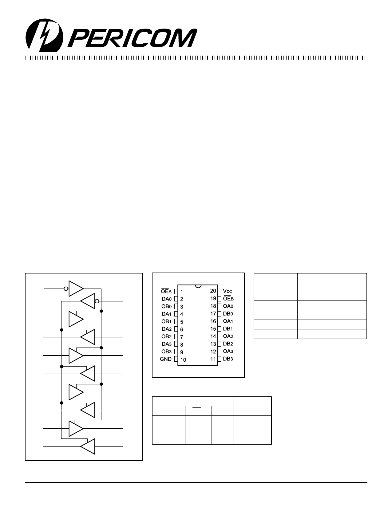
Logic Block Diagram
OEA
DA0
OB0
DA1
OB1
DA2
OB2
DA3
OB3
Pin Configuration
OEB
20-PIN
OA0
L20
Q20
R20
DB0
S20
OA1
Pin Description
Pin Name
OEA, OEB
Dxx
Oxx
GND
VCC
Description
3-State Output Enable
Inputs (Active LOW)
Inputs
Outputs
Ground
Power
DB1
OA2 Truth Table(1)
Inputs
Outputs
DB2
OEA
OEB
DXX
OXX
L
L
L
L
OA3
L
L
H
H
H
H
X
Z
DB3
Note:
1. H = High Voltage Level, X = Don’t Care,
L = Low Voltage Level, Z = High Impedance
1
PS7067E 11/09/98
Share Link: 