NCP1216A 데이터 시트보기 (PDF) - ON Semiconductor
부품명
상세내역
일치하는 목록
NCP1216A Datasheet PDF : 18 Pages
| |||
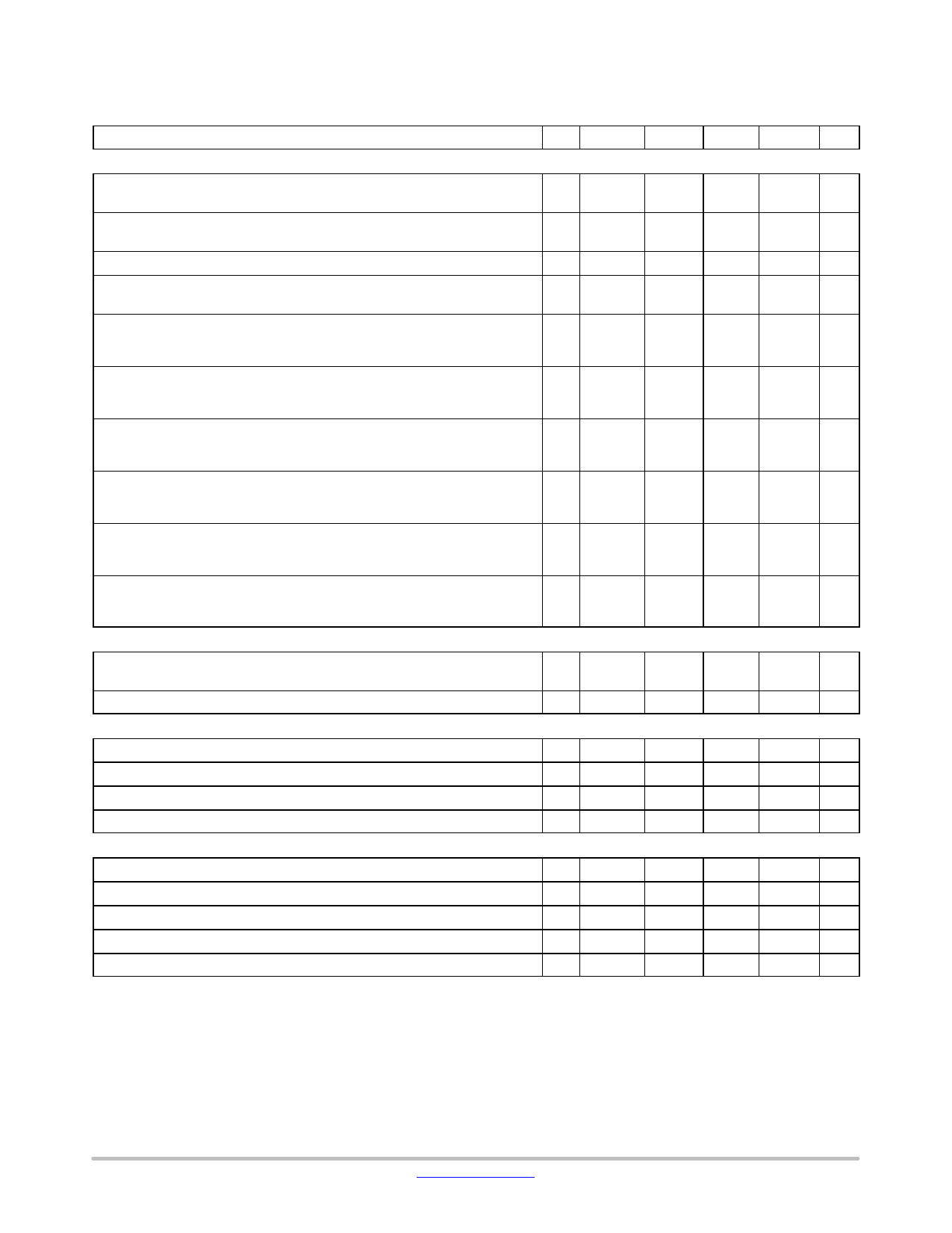
NCP1216, NCP1216A
ELECTRICAL CHARACTERISTICS
(For typical values TJ = 25°C, for min/max values TJ = −40°C to +125°C, Maximum TJ = 150°C, VCC = 11 V unless otherwise noted.)
Characteristic
Pin Symbol Min
Typ
Max Unit
DYNAMIC SELF−SUPPLY
VCC Increasing Level at which the Current Source Turns Off
6 VCCOFF 11.2
12.2
13.4
V
(Note 1)
VCC Decreasing Level at which the Current Source Turns On
6 VCCON
9.2
10.0
11.0
V
(Note 1)
VCC Decreasing Level at which the Latchoff Phase Ends
6 VCClatch
5.6
V
Internal IC Consumption, Latchoff Phase, VCC = 6.0 V
NCP1216 6
ICC3
NCP1216A
250
mA
320
Internal IC Consumption, No Output Load on Pin 5, FSW = 65 kHz
6
0°C ≤ TJ ≤ +125°C
−40°C ≤ TJ ≤ +125°C
Internal IC Consumption, No Output Load on Pin 5, FSW = 100 kHz
6
0°C ≤ TJ ≤ +125°C
−40°C ≤ TJ ≤ +125°C
Internal IC Consumption, No Output Load on Pin 5, FSW = 133 kHz
6
0°C ≤ TJ ≤ +125°C
−40°C ≤ TJ ≤ +125°C
Internal IC Consumption, 1.0 nF Output Load on Pin 5, FSW = 65 kHz
6
0°C ≤ TJ ≤ +125°C
−40°C ≤ TJ ≤ +125°C
Internal IC Consumption, 1.0 nF Output Load on Pin 5, FSW = 100 kHz
6
0°C ≤ TJ ≤ +125°C
−40°C ≤ TJ ≤ +125°C
Internal IC Consumption, 1.0 nF Output Load on Pin 5, FSW = 133 kHz
6
0°C ≤ TJ ≤ +125°C
−40°C ≤ TJ ≤ +125°C
INTERNAL STARTUP CURRENT SOURCE (TJ > 0°C)
High−voltage Current Source, VCC = 10 V
8
ICC1
mA
990
1110
1245
ICC1
mA
1025 1180
1285
ICC1
mA
1060 1200
1290
ICC2
mA
1.7
2.0
2.0
ICC2
mA
2.1
2.4
2.55
ICC2
mA
2.4
2.9
3.0
IC1
4.9
8.0
(Note 2)
11
mA
High−voltage Current Source, VCC = 0 V
DRIVE OUTPUT
8
IC2
9.0
mA
Output Voltage Rise−time @ CL = 1.0 nF, 10−90% of a 12 V Output Signal
Output Voltage Fall−time @ CL = 1.0 nF, 10−90% of a 12 V Output Signal
Source Resistance
Sink Resistance
CURRENT COMPARATOR (Pin 5 Unloaded)
5
Tr
60
5
Tf
20
5
ROH
15
20
5
ROL
5.0
10
ns
ns
35
W
18
W
Input Bias Current @ 1.0 V Input Level on Pin 3
3
IIB
0.02
mA
Maximum Internal Current Setpoint
3
ILimit
0.93
1.08
1.14
V
Default Internal Current Setpoint for Skip Cycle Operation
3
ILskip
330
mV
Propagation Delay from Current Detection to Gate OFF State
3
TDEL
80
130
ns
Leading Edge Blanking Duration
3
TLEB
220
ns
Product parametric performance is indicated in the Electrical Characteristics for the listed test conditions, unless otherwise noted. Product
performance may not be indicated by the Electrical Characteristics if operated under different conditions.
1. VCCOFF and VCCON min−max always ensure an hysteresis of 2.0 V.
2. Minimum value for TJ = 125°C.
www.onsemi.com
4
Share Link: 