NCP1216AD100R2G(2010) 데이터 시트보기 (PDF) - ON Semiconductor
부품명
상세내역
일치하는 목록
NCP1216AD100R2G
(Rev.:2010)
(Rev.:2010)
ON Semiconductor

NCP1216AD100R2G Datasheet PDF : 18 Pages
| |||
NCP1216, NCP1216A
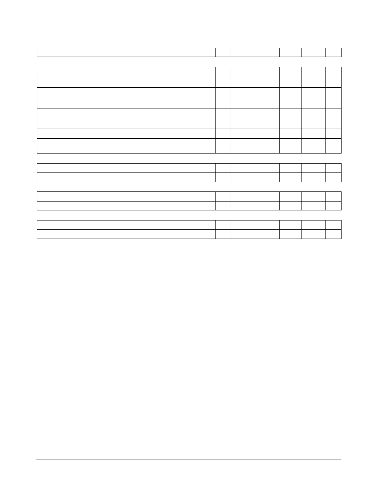
ELECTRICAL CHARACTERISTICS (continued) (For typical values TJ = 25°C, for min/max values TJ = 0°C to +125°C, Maximum
TJ = 150°C, VCC = 11 V unless otherwise noted.)
Characteristic
Pin Symbol Min
Typ
Max Unit
INTERNAL OSCILLATOR (VCC = 11 V, Pin 5 Loaded by 1.0 kW)
Oscillation Frequency, 65 kHz Version
Oscillation Frequency, 100 kHz Version
Oscillation Frequency, 133 kHz Version
Built−in Frequency Jittering in Percentage of fOSC
Maximum Duty−Cycle
NCP1216
NCP1216A
fOSC
fOSC
fOSC
fjitter
Dmax
58.5
65
71.5 kHz
90
100
110 kHz
120
133
146 kHz
±4.0
%
69
75
81
%
42
46.5
50
FEEDBACK SECTION (VCC = 11 V, Pin 5 Loaded by 1.0 kW)
Internal Pullup Resistor
Pin 2 (FB) to Internal Current Setpoint Division Ratio
SKIP CYCLE GENERATION
2
Rup
−
Iratio
20
kW
3.3
Default Skip Mode Level
Pin 1 Internal Output Impedance
INTERNAL RAMP COMPENSATION
1
Vskip
0.9
1.1
1.26
V
1
Zout
25
kW
Internal Ramp Level @ 25°C (Note 4)
Internal Ramp Resistance to CS Pin
4. A 1.0 MW resistor is connected to the ground for the measurement.
3
Vramp
2.6
2.9
3.2
V
3
Rramp
19
kW
http://onsemi.com
5
Share Link: