NCP1216AD100R2G(2010) 데이터 시트보기 (PDF) - ON Semiconductor
부품명
상세내역
일치하는 목록
NCP1216AD100R2G
(Rev.:2010)
(Rev.:2010)
ON Semiconductor

NCP1216AD100R2G Datasheet PDF : 18 Pages
| |||
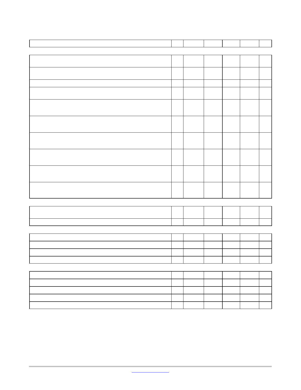
NCP1216, NCP1216A
ELECTRICAL CHARACTERISTICS (For typical values TJ = 25°C, for min/max values TJ = 0°C to +125°C, Maximum TJ = 150°C,
VCC = 11 V unless otherwise noted.)
Characteristic
Pin Symbol Min
Typ
Max Unit
DYNAMIC SELF−SUPPLY
VCC Increasing Level at which the Current Source Turns Off
6 VCCOFF 11.2
12.2
13.4
V
(Note 1)
VCC Decreasing Level at which the Current Source Turns On
6 VCCON
9.2
10.0
11.0
V
(Note 1)
VCC Decreasing Level at which the Latchoff Phase Ends
Internal IC Consumption, No Output Load on Pin 5, FSW = 65 kHz
6 VCClatch
6
ICC1
5.6
V
990
1110 mA
(Note 2)
Internal IC Consumption, No Output Load on Pin 5, FSW = 100 kHz
6
ICC1
1025 1180 mA
(Note 2)
Internal IC Consumption, No Output Load on Pin 5, FSW = 133 kHz
6
ICC1
1060 1200 mA
(Note 2)
Internal IC Consumption, 1.0 nF Output Load on Pin 5, FSW = 65 kHz
6
ICC2
1.7
2.0 mA
(Note 2)
Internal IC Consumption, 1.0 nF Output Load on Pin 5, FSW = 100 kHz
6
ICC2
2.1
2.4 mA
(Note 2)
Internal IC Consumption, 1.0 nF Output Load on Pin 5, FSW = 133 kHz
6
ICC2
2.4
2.9 mA
(Note 2)
Internal IC Consumption, Latchoff Phase, VCC = 6.0 V
NCP1216 6
ICC3
NCP1216A
250
mA
320
INTERNAL STARTUP CURRENT SOURCE (TJ > 0°C)
High−voltage Current Source, VCC = 10 V
8
IC1
4.9
8.0
(Note 3)
11
mA
High−voltage Current Source, VCC = 0 V
DRIVE OUTPUT
8
IC2
9.0
mA
Output Voltage Rise−time @ CL = 1.0 nF, 10−90% of a 12 V Output Signal
Output Voltage Fall−time @ CL = 1.0 nF, 10−90% of a 12 V Output Signal
Source Resistance
Sink Resistance
CURRENT COMPARATOR (Pin 5 Unloaded)
5
Tr
60
5
Tf
20
5
ROH
15
20
5
ROL
5.0
10
ns
ns
35
W
18
W
Input Bias Current @ 1.0 V Input Level on Pin 3
Maximum Internal Current Setpoint
Default Internal Current Setpoint for Skip Cycle Operation
Propagation Delay from Current Detection to Gate OFF State
Leading Edge Blanking Duration
1. VCCOFF and VCCON min−max always ensure an hysteresis of 2.0 V.
2. Maximum value at TJ = 0°C.
3. Minimum value for TJ = 125°C.
3
IIB
0.02
mA
3
ILimit
0.93
1.08
1.14
V
3
ILskip
330
mV
3
TDEL
80
130
ns
3
TLEB
220
ns
http://onsemi.com
4
Share Link: