NCP1217A(2004) 데이터 시트보기 (PDF) - ON Semiconductor
부품명
상세내역
일치하는 목록
NCP1217A
(Rev.:2004)
(Rev.:2004)
ON Semiconductor

NCP1217A Datasheet PDF : 18 Pages
| |||
NCP1217, NCP1217A
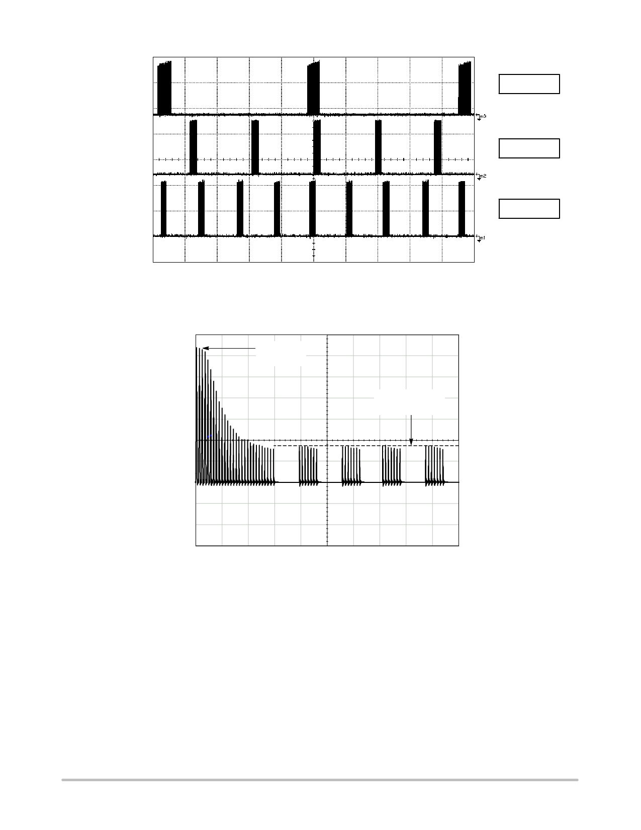
Power P1
Power P2
Power P3
Figure 20. Output Pulses at Various Power Levels (X = 5.0 ms/div) P1 t P2 t P3
300 M
200 M
100 M
0
MAX PEAK
CURRENT
SKIP CYCLE
CURRENT LIMIT
315.40 U 882.70 U 1.450 M
2.017 M
2.585 M
Figure 21. The Skip Cycle Takes Place at Low Peak Currents which Guarantees Noise−Free Operation
Sufficient margin shall be kept between normal Pin1 level and the latchoff point in order to avoid false triggering.
Ramp Compensation
Ramp compensation is a known mean to cure
subharmonic oscillations. These oscillations take place at
half the switching frequency and occur only during
Continuous Conduction Mode (CCM) with a duty−cycle
greater than 50%. To lower the current loop gain, one usually
injects between 50 and 100% of the inductor down−slope.
Figure 22 depicts how internally the ramp is generated.
http://onsemi.com
11
Share Link: