SL74HC393 데이터 시트보기 (PDF) - System Logic Semiconductor
부품명
상세내역
일치하는 목록
SL74HC393
System Logic Semiconductor

SL74HC393 Datasheet PDF : 7 Pages
| |||
SL74HC393
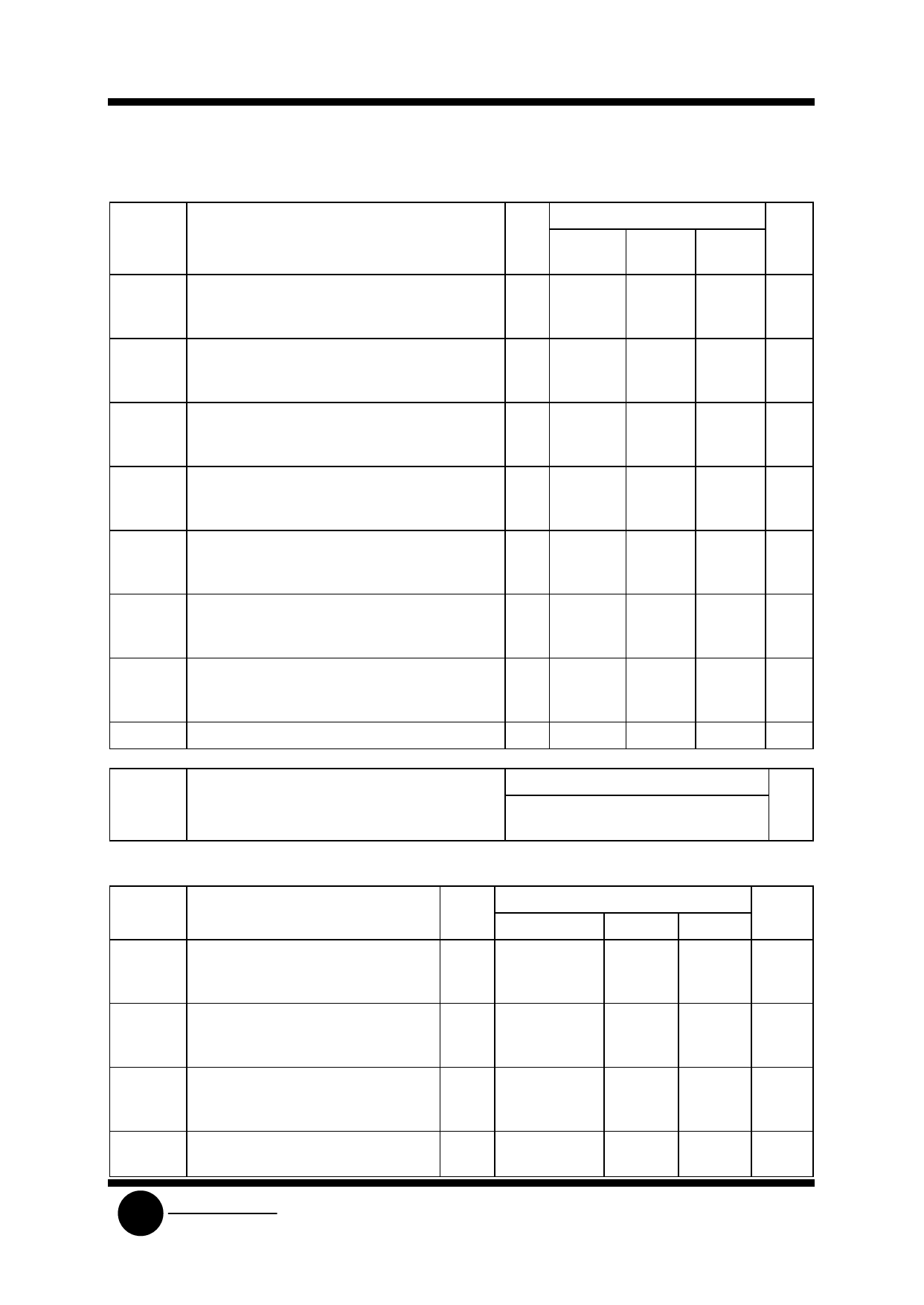
AC ELECTRICAL CHARACTERISTICS(CL=50pF,Input tr=tf=6.0 ns)
Symbol
Parameter
fmax Maximum Clock Frequency (50% Duty Cycle)
(Figures 1 and 3)
tPLH, tPHL Maximum Propagation Delay, Clock to Q1
(Figures 1 and 3)
tPLH, tPHL Maximum Propagation Delay, Clock to Q2
(Figures 1 and 3)
tPLH, tPHL Maximum Propagation Delay, Clock to Q3
(Figures 1 and 3)
tPLH, tPHL Maximum Propagation Delay, Clock to Q4
(Figures 1 and 3)
tPHL Maximum Propagation Delay, Reset to any Q
(Figures 2 and 3)
tTLH, tTHL Maximum Output Transition Time, Any Output
(Figures 1 and 3)
CIN
Maximum Input Capacitance
VCC
Guaranteed Limit
V 25 °C to ≤85°C ≤125°C Unit
-55°C
2.0
5.4
4.5
27
6.0
32
4.4
3.6 MHz
22
18
26
21
2.0
120
150
180 ns
4.5
24
30
36
6.0
20
26
31
2.0
190
240
285 ns
4.5
38
48
57
6.0
32
41
48
2.0
240
300
360 ns
4.5
48
60
72
6.0
41
51
61
2.0
290
365
435 ns
4.5
58
73
87
6.0
49
62
74
2.0
165
205
250 ns
4.5
33
41
50
6.0
28
35
43
2.0
75
4.5
15
6.0
13
95
110 ns
19
22
16
19
-
10
10
10
pF
Power Dissipation Capacitance (Per Counter)
CPD Used to determine the no-load dynamic power
consumption: PD=CPDVCC2f+ICCVCC
Typical @25°C,VCC=5.0 V
40
TIMING REQUIREMENTS(CL=50pF,Input tr=tf=6.0 ns)
Symbol
trec
Parameter
Minimum Recovery Time, Reset
Inactive to Clock (Figure 2)
tw
Minimum Pulse Width, Clock (Figure
1)
tw
Minimum Pulse Width, Set
(Figure 2)
tr, tf Maximum Input Rise and Fall Times
(Figure 1)
SLS
System Logic
Semiconductor
VCC
Guaranteed Limit
V 25 °C to-55°C ≤85°C ≤125°C
2.0
50
4.5
10
6.0
9
65
75
13
15
11
13
2.0
80
4.5
16
6.0
14
100
120
20
24
17
20
2.0
125
4.5
25
6.0
21
155
190
31
38
26
32
2.0
1000
4.5
500
6.0
400
1000
1000
500
500
400
400
pF
Unit
ns
ns
ns
ns
Share Link: