PCK2011DB 데이터 시트보기 (PDF) - Philips Electronics
부품명
상세내역
일치하는 목록
PCK2011DB Datasheet PDF : 11 Pages
| |||
Philips Semiconductors
Direct Rambus™ Clock Generator
Preliminary specification
PCK2011
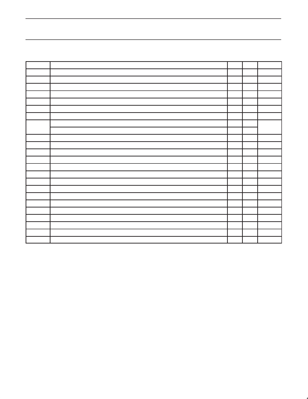
Table 3. DC DEVICE CHARACTERISTICS
Symbol Parameter
Min Max Unit
V DD
Supply voltage
3.135 3.465 V
TA
Ambient operating temperature
0
70
°C
tCYCLE ,IN
tJ,IN
DCIN
fM,IN 3
PM,IN
PM,IN 3
Refclk Input cycle time
Input Cycle-to-cycle jitter1
Input duty cycle over 10,000 cycles
Input frequency of modulation
Modulation index
Modulation index for triangular modulation
Modulation index for non-triangular modulation4
10
–
40%
30
0.25
–
–
40
250
60%
33
0.5
0.6
0.54
ns
ps
tCYCLE
kHz
%
%
tCYCLE,PD
Phase Detector input cycle time at PclkM & SynClkN
30
100 ns
tERR,INIT
Initial Phase error at Phase Detector inputs (Required range of Phase Aligner)
–0.5 0.5
tCYCLE,PD
DCIN,PD
Phase Detector input duty cycle over 10,000 cycles
25% 75% tCYCLE,PD
tIR , tIF
CIN,PD
∆CIN,PD
CIN,CMOS
Input slew rate (measured at 20% – 80% of input voltage) for PclkM, SynClkN, and Refclk
Input capacitance at PclkM, SynClkN, and Refclk2
Input capacitance matching at PclkM and SynClkN2
Input capacitance at CMOS pins2
1
4
V/ns
–
7
pF
–
0.5 pF
–
10
pF
VIL
Input (CMOS) signal low voltage
–
0.3 Vdd
VIH
Input (CMOS) signal high voltage
0.7 –
Vdd
VIL,R
Refclk input low voltage
–
0.3 VddI,R
VIH,R
Refclk input high voltage
0.7 –
VddI,R
VIL,PD
Input signal low voltage for PD inputs and StopB
–
0.3 VddI,PD
VIH,PD
Input signal high voltage for PD inputs and StopB
0.7 –
VddI,PD
VDDI,R
Input supply reference for Refclk
1.3 3.3 V
VDDI,PD
Input supply reference for PD inputs
1.3 3.3 V
NOTES:
1. Refclk jitter measured at VDDI,R(nom)/2
2. Capacitance measured at Freq = 1MHz, DC bias = 0.9V, and VAC < 100mV
3. If the input modulation is used, input modulation is allowed but not required.
4. The amount of allowed spreading for any non-triangular modulation is determined by the induced downstream tracking skew, which cannot
exceed the skew generated by the specified 0.6% triangular modulation. Typically, the amount of allowed non-triangular modulation is about
0.5%.
1999 Jan 19
7
Share Link: 