5503DCR 데이터 시트보기 (PDF) - TDK Corporation
부품명
상세내역
일치하는 목록
5503DCR Datasheet PDF : 11 Pages
| |||
5503 DCR
Direct Conversion Receiver
PIN DESCRIPTIONS
ANALOG PINS
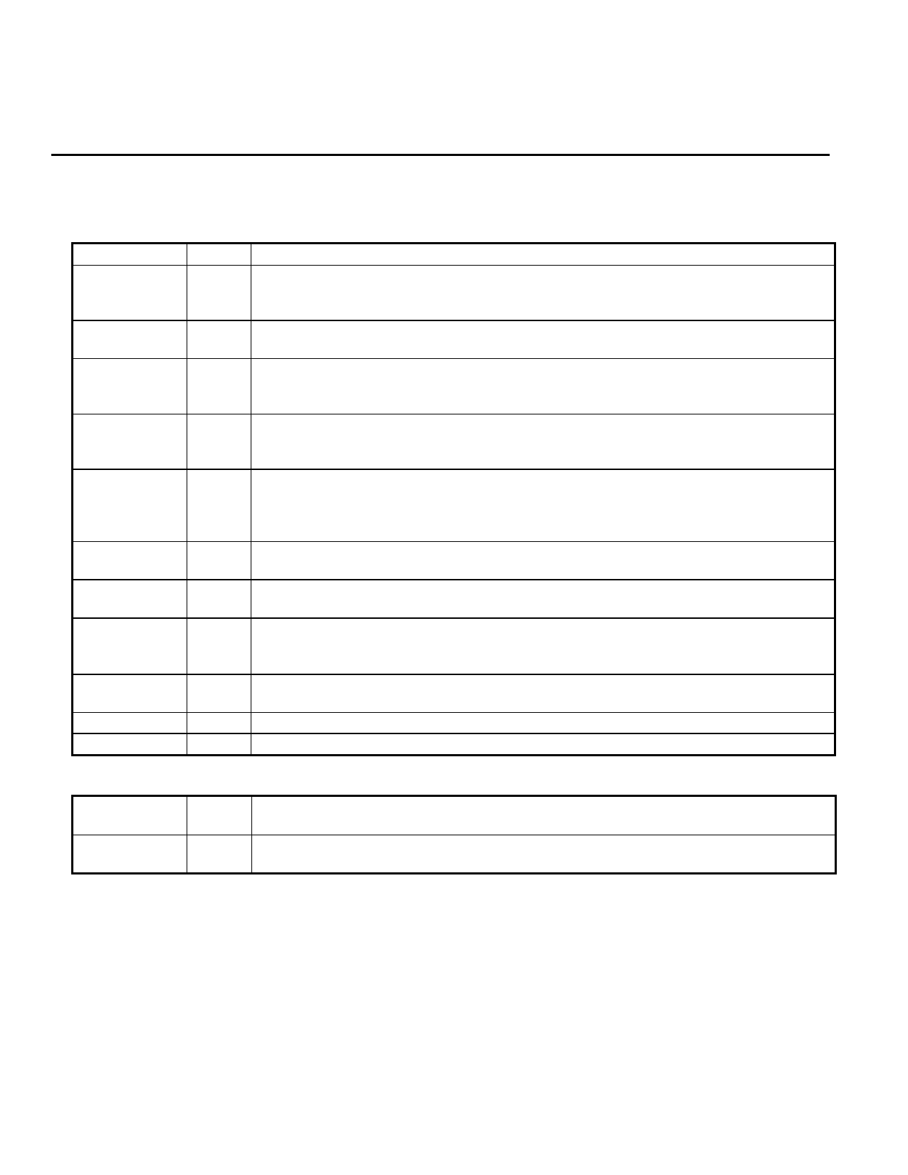
NAME
RFP, RFN
TYPE
I
AGC
I
Eop, Filp
I/O
Eon, Filn
I/O
XTLP, XTLN
I
IO2, QO2
O
IO1, QO1
O
IIN, QIN
I
Rxt
I
RSHP, RSHN
I
RSLP, RSLN
I
DESCRIPTION
RF inputs: balanced differential inputs to the receiver. The input signals placed on this
line are amplified with a variable gain amplifier before being passed to the I/Q
demodulator.
Automatic gain control input. A voltage from 0 to 4 volts on this pin varies the input
amplifier gain from minimum to maximum. The gain increase is 22 dB typical
External loop filter interface. Eop drives the base of an external common emitter
transistor. Filp is the feedback input from the loop filter capacitor. This output is used
for a negative VCO gain characteristic.
External loop filter interface. Eon drives the base of an external common emitter
transistor. Filn is the feedback input from the loop filter capacitor. This output is used
for a positive VCO gain characteristic.
Reference crystal input. An external crystal connected between these pins
establishes the reference frequency for the PLL synthesizer. The crystal frequency
must be 8 MHz and have an ESR of less than 100 Ohms. Following this oscillator is a
programmable divider which establishes the synthesizer step size.
Baseband outputs. These typically drive an A/D converter prior to digital
demodulation and processing.
I and Q channel outputs to external low pass filter. An external series resistor is
connected between this output and the filter to provide the source match.
I and Q channel inputs from external low pass filter. These are high impedance inputs
( >1000Ω). The low pass filter must be designed for a low input and high output
impedance.
External reference resistor. This resistor is connected to ground and must be 7.68k
±1% . It is used as a reference for internal bias currents.
High range VCO resonator inputs
Low range VCO resonator inputs
DIGITAL PINS
Din
I/O I2C data. This signal is connected to the I2C internal block. An external resistor
(typically 2.2 kΩ) is connected between Din and Vcc for proper operation
Dclk
I
I2C clock Input: Dclk should nominally be a square wave with a maximum frequency
of 400kHz. SCL is generated by the system I2C master
4
Share Link: 