W144 데이터 시트보기 (PDF) - SpectraLinear Inc
부품명
상세내역
일치하는 목록
W144 Datasheet PDF : 13 Pages
| |||
W144
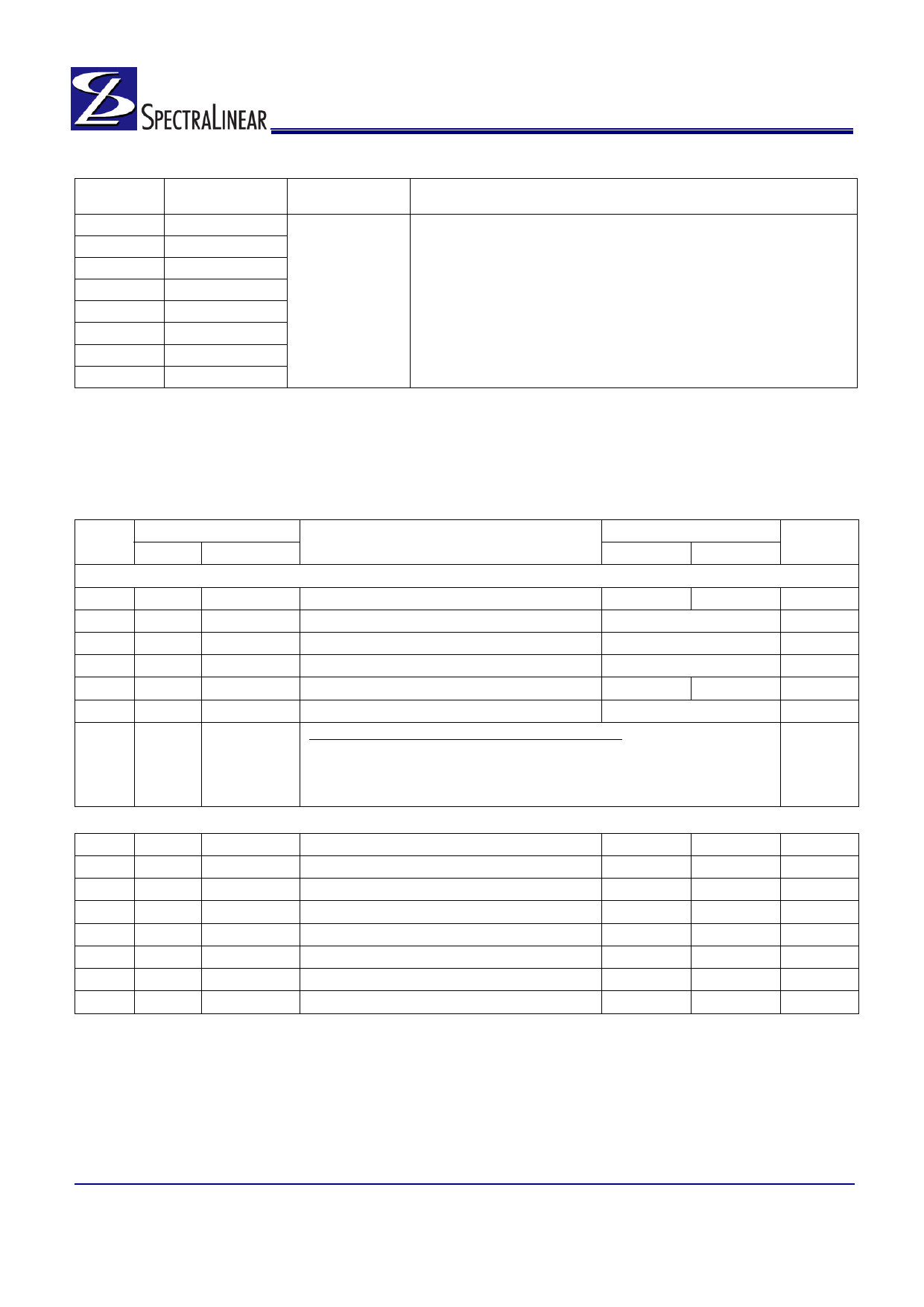
Table 4. Byte Writing Sequence (continued)
Byte
Sequence
4
5
Byte Name
Data Byte 0
Data Byte 1
Bit Sequence
Refer to Table 5
6
Data Byte 2
7
Data Byte 3
8
Data Byte 4
9
Data Byte 5
10
Data Byte 6
11
Data Byte 7
Byte Description
The data bits in Data Bytes 0–7 set internal W144 registers that control
device operation. The data bits are only accepted when the Address Byte
bit sequence is 11010010, as noted above. For description of bit control
functions, refer to Table 5, Data Byte Serial Configuration Map.
Writing Data Bytes
Each bit in Data Bytes 0–7 controls a particular device function
except for the “reserved” bits, which must be written as a logic
0. Bits are written MSB (most significant bit) first, which is bit 7.
Table 5 gives the bit formats for registers located in Data Bytes
0–7.
Table 5. Data Bytes 0-7 Serial Configuration Map
Table 6 details additional frequency selections that are
available through the serial data interface.
Table 7 details the select functions for Byte 0, bits 1 and 0.
Affected Pin
Bit Control
Bit(s) Pin No. Pin Name
Control Function
0
1
Default
Data Byte 0
7
–
–
(Reserved)
–
–
0
6
–
–
SEL_2
See Table 6
0
5
–
–
SEL_1
See Table 6
0
4
–
–
SEL_0
See Table 6
0
3
–
–
Hardware/Software Frequency Select
Hardware Software
0
2
–
–
SEL_3
See Table 6
0
1–0
–
–
Bit 1Bit 0Function (See Table 7 for function details)
00
00Normal Operation
01(Reserved)
10Spread Spectrum On
11All Outputs Three-stated
Data Byte 1
7
–
6
–
5
–
4
–
3
40
2
–
1
43
0
44
–
–
–
–
SDRAM_F
–
CPU1
CPU_F
(Reserved)
(Reserved)
(Reserved)
(Reserved)
Clock Output Disable
(Reserved)
Clock Output Disable
Clock Output Disable
–
–
0
–
–
0
–
–
0
–
–
0
Low
Active
1
–
–
0
Low
Active
1
Low
Active
1
Rev 1.0, November 21, 2006
Page 6 of 13
Share Link: 