W150 데이터 시트보기 (PDF) - Cypress Semiconductor
부품명
상세내역
일치하는 목록
W150 Datasheet PDF : 15 Pages
| |||
PRELIMINARY
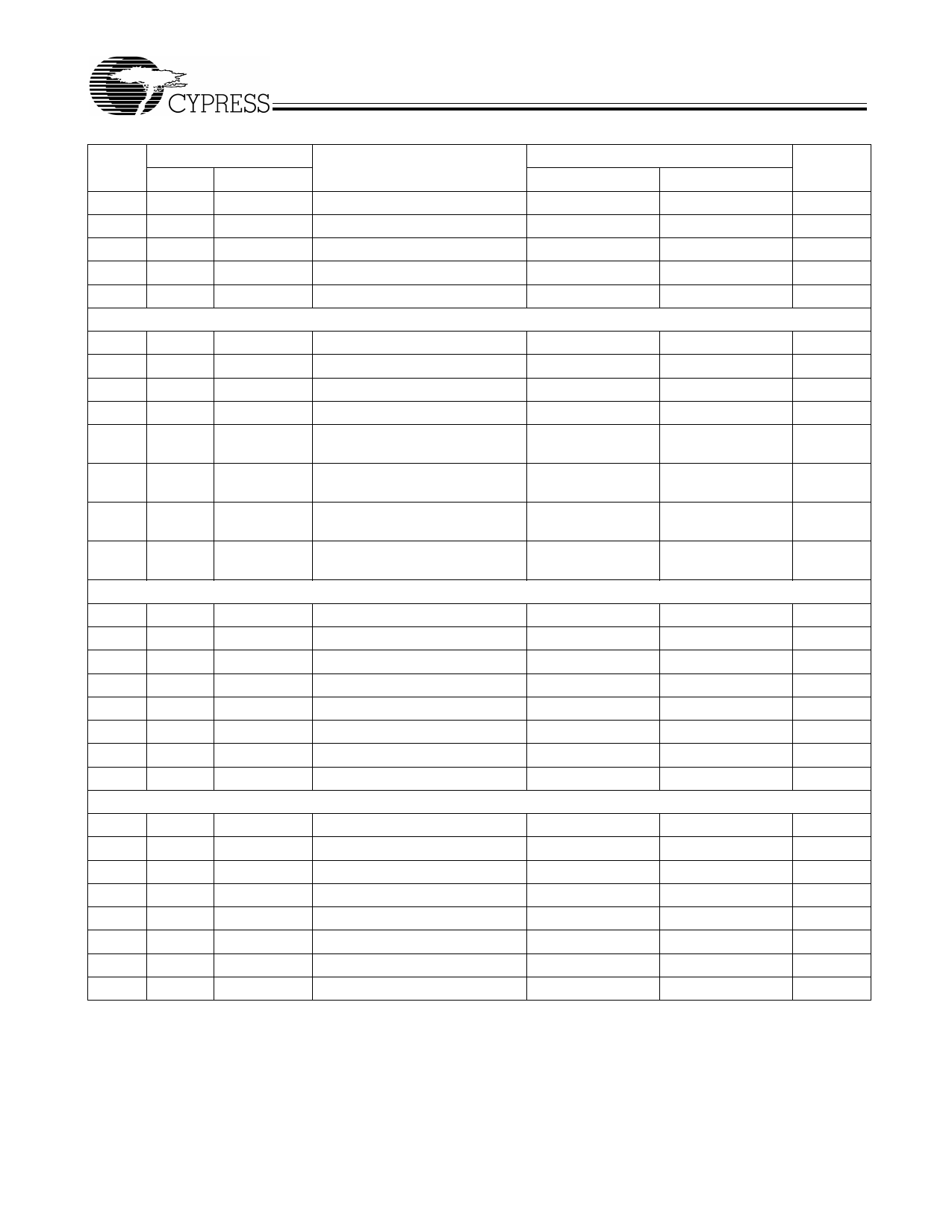
Table 5. Data Bytes 0–5 Serial Configuration Map (continued)
Affected Pin
Bit(s) Pin No. Pin Name
Control Function
4
14
PCI4
Clock Output Disable
3
13
PCI3
Clock Output Disable
2
12
PCI2
Clock Output Disable
1
11
PCI1
Clock Output Disable
0
9
PCI0
Clock Output Disable
Data Byte 3
7
–
–
(Reserved)
6
–
–
(Reserved)
5
29
48MHz Clock Output Disable
4
30
24MHz Clock Output Disable
3
33, 32, SDRAM12:15 Clock Output Disable
25, 24
2
22, 21, SDRAM8:11 Clock Output Disable
19, 18
1
39, 38, SDRAM4:7 Clock Output Disable
36, 35
0
44, 43, SDRAM0:3 Clock Output Disable
41, 40
Data Byte 4
7
–
–
(Reserved)
6
–
–
(Reserved)
5
–
–
(Reserved)
4
–
–
(Reserved)
3
–
–
(Reserved)
2
–
–
(Reserved)
1
–
–
(Reserved)
0
–
–
(Reserved)
Data Byte 5
7
–
–
(Reserved)
6
–
–
(Reserved)
5
54
IOAPIC_F Disabled
4
55
IOAPICO Disabled
3
–
–
(Reserved)
2
–
–
(Reserved)
1
2
REF1
Clock Output Disable
0
3
REF0
Clock Output Disable
Bit Control
0
1
Low
Active
Low
Active
Low
Active
Low
Active
Low
Active
–
–
–
–
Low
Active
Low
Active
Low
Active
Low
Active
Low
Active
Low
Active
–
–
–
–
–
–
–
–
–
–
–
–
–
–
–
–
–
–
–
–
Low
Active
Low
Active
–
–
–
–
Low
Active
Low
Active
W150
Default
1
1
1
1
1
0
0
1
1
1
1
1
1
0
0
0
0
0
0
0
0
0
0
1
1
0
0
1
1
Document #: 38-07177 Rev. *B
Page 7 of 15
Share Link: 