HSP50016-EV 데이터 시트보기 (PDF) - Intersil
부품명
상세내역
일치하는 목록
HSP50016-EV Datasheet PDF : 18 Pages
| |||
HSP50016-EV
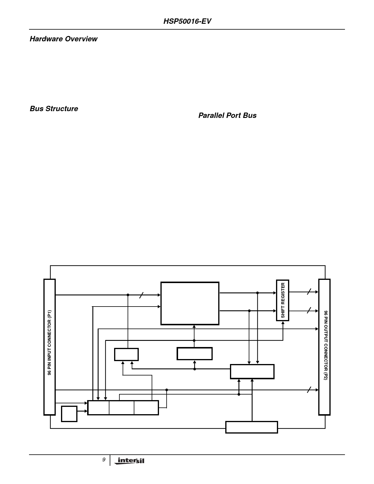
Hardware Overview
The HSP50016-EV was designed to facilitate prototyping
with the HSP50016 Digital Down Converter. It can be used in
a stand alone mode, in conjunction with other Intersil
evaluation boards, or be inserted into a card cage and
operate as a part of a larger system. The following
description of the board references both the Block Diagram
in Figure 6 and the Schematic Diagrams, which are included
at the back of this manual.
Bus Structure
The HSP50016-EV utilizes a set of busses for DDC input,
output and control as shown in Figure 6. The input and
output busses connect the DDC to the outside world through
96 Pin DIN connectors conforming to the VME J2/P2
Connector Standard. DDC control information is provided
either by control registers down loaded via the parallel port
of a PC or from the 96 Pin DIN connectors
The DDC’s input data bus, DIN0-15, is driven from the 96 Pin
DIN connector P1 (Pinout shown in Table 3). DIN0-15 may
be driven by Registers U12 and U13 which have been down
loaded with data through the Parallel Port Bus. The source of
the input data is selected by jumper JP5. Installing the
shorting jumper on JP5 selects the PC as the data source.
Removing the jumper puts the registers driving the DIN0-15
bus in a high impedance state so that the input data can be
driven from P1.
The control lines of the DDC and the board are driven by the
outputs of the Control Registers (U11, U16). These registers
are down loaded with data via the Parallel Port Bus or
through the PCD0-7 lines on P1 or P2. when the board is
controlled through the 96 Pin DIN connectors, the user must
emulate the operation of the PC interface. A description of
this operation is given below in the section describing the
Parallel Port Bus.
The DDC output is available through three different paths: It
is connected to the Select line of the PC Parallel Port
through the eight to one multiplexer U6; it is connected to the
96 Pin DIN connector P2 through the buffer U1; finally, it is
converted to parallel data by the Shift Registers U2-5 and
driven out on P2. The mapping for P2 is given in Table 4.
Parallel Port Bus
The Parallel Port Bus carries the write only parallel data and
signals required to support bidirectional data transfers
between the HSP50016-EV and the parallel port of the PC.
This bus contains eight data lines, PCD0-7, two control lines,
PCWR0-1, and the serial output line PCRD1. The control
and data lines are used to down load data into the on board
registers of the HSP50016-EV. The serial output line carries
the DDC output data back to the PC.
The Parallel Port Bus is attached to the PC by connecting
the ribbon cable provided to the PC's parallel port and to the
26 pin connector J1 on the DDC Evaluation Board. The
ribbon cable maps the Parallel Port Bus signals to the PC's
parallel port as shown in Table 5.
The Parallel Port Bus is brought out through each of the 96
Pin DIN connectors (P1, P2) so that multiple Intersil
evaluation boards can be daisy chained. This allows all of
the evaluation boards in the chain to be controlled through a
single board which has been connected to a host PC.
INPUT BUS 1
16
(DIN0-15)
CLK IN
HSP50016JC-52
I0-15 16
Q0-15 16
EXT CLK
OSC
CONTROL BUS
CLK OUT
INPUT
REG 1
CONTROL
REG
PARALLEL PORT
INTERFACE
PARALLEL PORT BUS
CLK ADDRESS OUTPUT
SELECT SELECT ENABLE
CONFIGURATION JUMPER FIELD (JP1-3, 5-18)
13
PARALLEL PORT CONNECTOR
(J1)
26 PIN CONNECTOR
FIGURE 6. BLOCK DIAGRAM OF HSP50016-EV
9
Share Link: 