U630H16P 데이터 시트보기 (PDF) - Simtek Corporation
부품명
상세내역
일치하는 목록
U630H16P Datasheet PDF : 17 Pages
| |||

Obsolete - Not Recommended for New Designs
U630H16P
HardStore 2K x 8 nvSRAM
Features
Description
• High-performance CMOS nonvo-
latile static RAM 2048 x 8 bits
• 35 ns Access Times
• 20 ns Output Enable Access
Times
• Hardware and Software STORE
Initiation
(STORE Cycle Time < 10 ms)
• Automatic STORE Timing
• 106 STORE cycles to EEPROM
• 100 years data retention in
EEPROM
• Automatic RECALL on Power Up
• Hardware and Software RECALL
Initiation
(RECALL Cycle Time < 20 μs)
• Unlimited RECALL cycles from
EEPROM
• Unlimited Read and Write to
SRAM
• Single 5 V ± 10 % Operation
• Operating temperature ranges:
0 to 70 °C
-40 to 85 °C
• QS 9000 Quality Standard
• ESD characterization according
MIL STD 883C M3015.7-HBM
(classification see IC Code
Numbers)
• Package: PLCC32
The U630H16P has two separate
modes of operation: SRAM mode
and nonvolatile mode, determined
by the state of the NE pin.
In SRAM mode, the memory ope-
rates as an ordinary static RAM. In
nonvolatile operation, data is trans-
ferred in parallel from SRAM to
EEPROM or from EEPROM to
SRAM. In this mode SRAM
functions are disabled.
The U630H16P is a fast static RAM
(35 ns), with a nonvolatile electri-
cally erasable PROM (EEPROM)
element incorporated in each static
memory cell. The SRAM can be
read and written an unlimited num-
ber of times, while independent
nonvolatile data resides in
EEPROM. Data transfers from the
SRAM to the EEPROM (the
STORE operation), or from the
EEPROM to the SRAM (the
RECALL operation) are initiated
through the state of the NE pin or
through software sequences.
The U630H16P combines the high
performance and ease of use of a
fast SRAM with nonvolatile data
integrity.
Once a STORE cycle is initiated,
further input or output are disabled
until the cycle is completed.
Because a sequence of addresses
is used for STORE initiation, it is
important that no other read or
write accesses intervene in the
sequence or the sequence will be
aborted.
Internally, RECALL is a two step
procedure. First, the SRAM data is
cleared and second, the nonvola-
tile information is transferred into
the SRAM cells.
The RECALL operation in no way
alters the data in the EEPROM
cells. The nonvolatile data can be
recalled an unlimited number of
times.
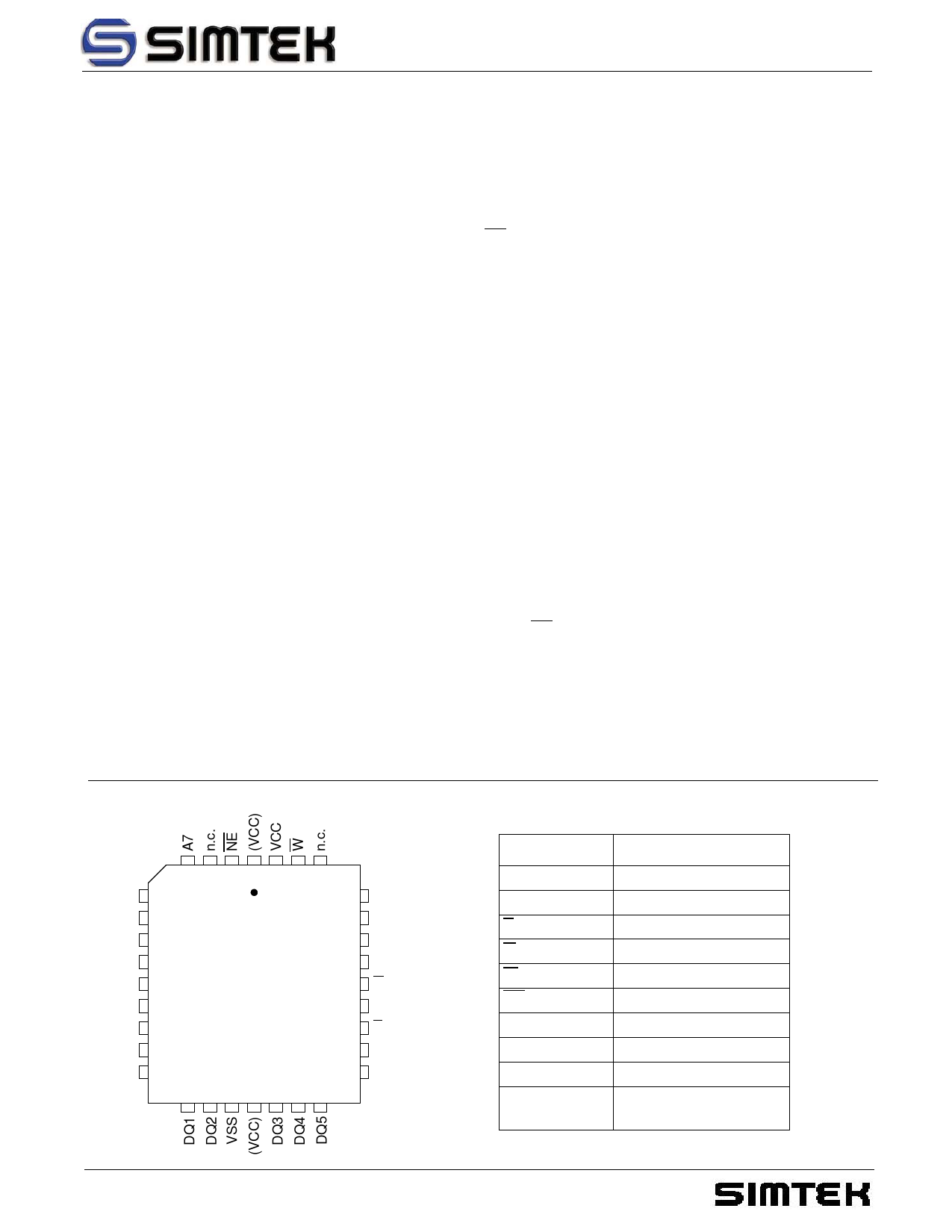
Pin Configuration
A6
A5
A4
A3
A2
A1
A0
n.c.
DQ0
4 3 2 1 32 31 30
5
29
6
28
7
27
8
26
9
25
10
24
11
23
12
22
13
21
14 15 16 17 18 19 20
A8
A9
n.c.
n.c.
G
A10
E
DQ7
DQ6
Top View
March 31, 2006
STK Control #ML0037
Pin Description
Signal Name
A0 - A10
DQ0 - DQ7
E
G
W
NE
VCC
VSS
n.c.
(VCC)
Signal Description
Address Inputs
Data In/Out
Chip Enable
Output Enable
Write Enable
Nonvolatile Enable
Power Supply Voltage
Ground
not connected
Power Supply Voltage
(optional)
1
Rev 1.0