IDT72605(2013) 데이터 시트보기 (PDF) - Integrated Device Technology
부품명
상세내역
일치하는 목록
IDT72605 Datasheet PDF : 17 Pages
| |||
IDT72605/72615 CMOS SYNCBiFIFO™
256 x 18x 2 and 512 x 18 x 2
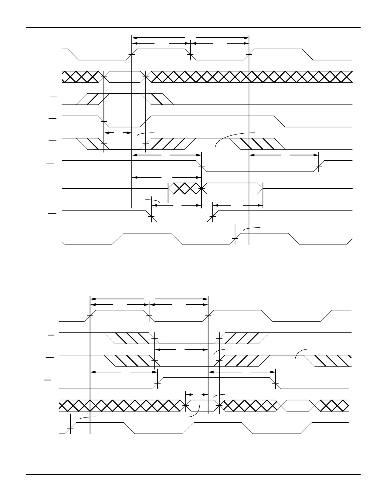
CLKB
R/WB
ENB
DB0-DB17
CLKA
tCS
tDS
D0 (First valid write)
D1
tSKEW1
tFRL
(1)
A0, A1, A2
R/WA
CSA, ENA
EFBA
DA0-DA17
OEA
tEF
tOLZ
tCS
tA
tOE
NOTE:
1. When tSKEW1 ≥ minimum specification, tFRL(Max.) = tCLK + tSKEW1
tSKEW1 < minimum specification, tFRL(Max.) = 2tCLK + tSKEW1
The Latency Timing apply only at the Empty Boundary (EF = LOW).
INDUSTRIAL TEMPERATURE RANGE
D2
D3
tA
D0
D1
2704 drw 12
Figure 9. B→A First Data Word Latency after Reset for Simultaneous Read and Write
12
Share Link: 