24C16 데이터 시트보기 (PDF) - Turbo IC Inc
부품명
상세내역
일치하는 목록
24C16 Datasheet PDF : 8 Pages
| |||
Turbo IC, Inc.
24C16
CMOS I²C 2-WIRE BUS
16K ELECTRICALLY ERASABLE PROGRAMMABLE ROM
2K X 8 BIT EEPROM
FEATURES :
• Extended Power Supply Voltage
Single Vcc for Read and Programming
(Vcc = 2.7 V to 5.5 V)
• Low Power (Isb = 2µa @ 5.5 V)
• I²C Bus, 2-Wire Serial Interface
• Support Byte Write and Page Write (16 Bytes)
• Automatic Page write Operation (maximum 10 ms)
Internal Control Timer
Internal Data Latches for 16 Bytes
• Hardware Data Protection by Write Protect Pin
• High Reliability CMOS Technology with EEPROM Cell
Endurance : 1,000,000 Cycles
Data Retention : 100 Years
DESCRIPTION:
The Turbo IC 24C16 is a serial 16K EEPROM fabricated
with Turbo’s proprietary, high reliability, high performance
CMOS technology. It’s 16K of memory is organized as 2,048
x 8 bits. The memory is configured as 128 pages with each
page containing 16 bytes. This device offers significant ad-
vantages in low power and low voltage applications.
The Turbo IC 24C16 uses the I²C addressing protocol and
2-wire serial interface which includes a bidirectional serial
data bus synchronized by a clock. It offers a flexible byte
write and a faster 16-byte page write. The data in the upper
half of memory can be protected by a write protect pin.
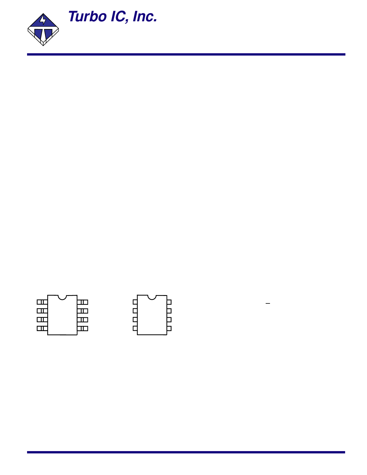
The Turbo IC 24C16 is assembled in either a 8-pin PDIP or
8-pin SOIC package. Pin #1, #2, and #3 are not connected
(NC). Pin #4 is the ground (Vss). Pin #5 is the serial data
(SDA) pin used for bidirectional transfer of data. Pin #6 is
the serial clock (SCL) input pin. Pin #7 is the write protect
(WP) input pin, and Pin #8 is the power supply (Vcc) pin.
PIN DESCRIPTION
NC
NC
NC
GND
1
8
2
7
3
6
4
5
VCC
WP
SCL
SDA
8 pin SOIC
All data is serially transmitted in bytes (8 bits) on the SDA
bus. To access the Turbo IC 24C16 (slave) for a read or
write operation, the controller (master) issues a start condi-
tion by pulling SDA from high to low while SCL is high. The
NC 1
NC 2
8 VCC master then issues the device address byte which consists
of 1010 (B10) (B9) (B8) (R/W). The most significant bits
7 WP (1010) are a device type code signifying an EEPROM de-
NC 3
6 SCL vice. The B[10:8] bits are the 3 most significant bits of the
GND 4 5 SDA memory address. The read/write bit determines whether to
do a read or write operation. After each byte is transmitted,
8 pin PDIP
the receiver has to provide an acknowledge by pulling the
SDA bus low on the ninth clock cycle. The acknowledge is a
handshake signal to the transmitter indicating a successful
data transmission.
PIN DESCRIPTION
WRITE PROTECT (WP)
When the write protect input is connected to Vcc,
the upper half of memory (400-7FFH) is protected
against write operations. For normal write opera-
tion, the write protect pin should be grounded.
When this pin is left unconnected, WP is inter-
preted as zero.
SERIAL DATA (SDA)
SDA is a bidirectional pin used to transfer data
in and out of the Turbo IC 24C16. The pin is an
open-drain output. A pullup resistor must be con-
nected from SDA to Vcc.
SERIAL CLOCK (SCL)
The SCL input synchronizes the data on the SDA
bus. It is used in conjunction with SDA to define
the start and stop conditions. It is also used in
conjunction with SDA to transfer data to and from
the Turbo IC 24C16.
1
Share Link: 