XRD6415 데이터 시트보기 (PDF) - Exar Corporation
부품명
상세내역
일치하는 목록
XRD6415 Datasheet PDF : 20 Pages
| |||
XRD6415
THEORY OF OPERATION
VIN Analog Input
This part has a switched capacitor, sampling input circuit.
The input impedance changes with the phase of the input
clock. VIN is sampled on the low to high clock transition
and the digital data updates on the low to high clock
transition. The diagram Figure 4. shows an equivalent
input circuit.
VDD
VIN
GND
100Ω CLK
18pF 100Ω
5pF
CLK
VRT + VRB +
1.5pF
CL
2
−
Figure 4. Equivalent Input Circuit
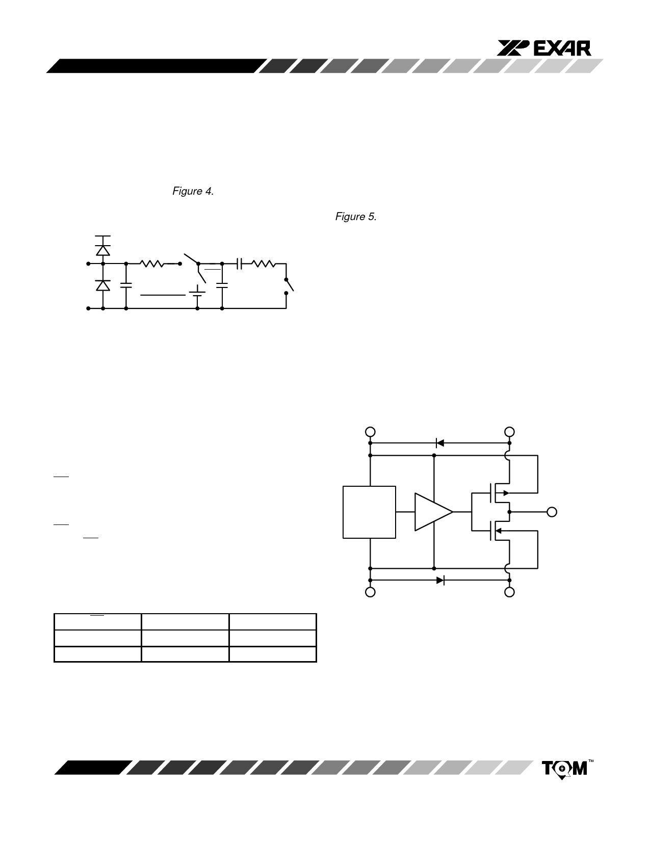
Logic Output Interface
The digital output drive circuitry of the XRD6415 was
designed to operate separately from the analog supplies.
The DVDD pin of the XRD6415 is a separate power supply
dedicated to the logic output drivers. DVDD is not
connected internally with any of the other power supplies.
Figure 5. illustrates the power supply circuitry of the
XRD6415.
DVDD and DGND connect directly to the digital logic
power of the user’s system isolating the analog and digital
power supplies and grounds. DGND is not common to the
XRD6415 substrate. The XRD6415 substrate is common
only to the packages’ GND pins. Best spectral
performance is obtained when DVDD is lowered to 3.3V.
See the power supply referencing section if VDD and
DVDD are powered separately.
OFW Overflow (Output)
This signal indicates when the Analog Input (VIN) goes
above VRT. The pin is normally at a low logic level. When
VIN > VRT, OFW will go high and the data bits (DB0 – DB9)
will show full scale (i.e. all 1s).
OE Output Enable (Input)
This signal controls the 3-state drivers on the digital
outputs DB0 – DB9 and OFW. During normal operation
OE should be held low so that all outputs are enabled.
When OE is driven high DB0 – DB9 and OFW go into high
impedance mode. This control operates asynchronous to
the clock and will only control the output drivers. The
internal output register will get updated if the clock is
running while the outputs are in three-state mode.
OE
DBO-DB9
OFW
0
Enabled
Enabled
1
Three-Stated
Three-Stated
Table 1. Output Enable
Source–body junction diode
VDD
between DVDD
DVDD
& VDD
A/D Circuit
DB(0-9)
& OFW
GND
Source–body junction
diode between DGND
& GND
DGND
Figure 5. XRD6415 ADC Power Supply
Circuit Allows Separate VDD & DVDD and
Separate GND & DGND
Rev. 1.00
10
Share Link: 