TDA9901TS 데이터 시트보기 (PDF) - Philips Electronics
부품명
상세내역
일치하는 목록
TDA9901TS Datasheet PDF : 20 Pages
| |||
Philips Semiconductors
Wideband differential digital controlled
variable gain amplifier
Product specification
TDA9901
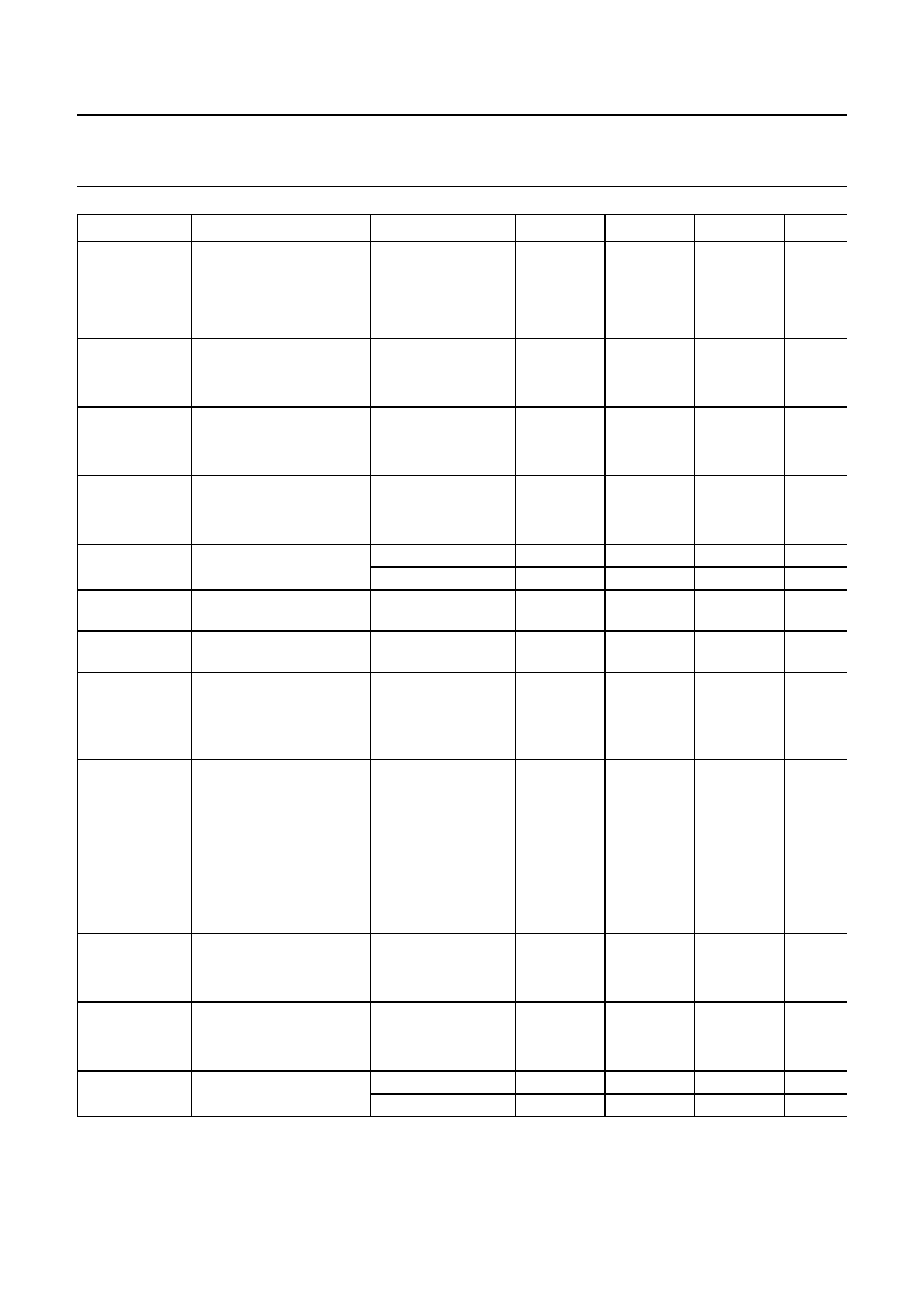
SYMBOL
tst
Gstep
G(min)
G(max)
∆G/∆T
|∆G/∆VDD|
∆Vi(offset)
F
Vn(o)(eq)
PSRR(VDDA)
PSRR(VDDD)
CMRR
PARAMETER
CONDITIONS
MIN.
settling time
gain step size
10 to 90% maximum −
output transition;
CL(max) = 5 pF on
each output;
Tamb = 25 °C
DC input
Tamb = 25 °C
5.88
all temperatures 5.6
minimum gain setting
DC input
Tamb = 25 °C
5.76
all temperatures 5.7
maximum gain setting DC input
Tamb = 25 °C
29.9
all temperatures 29.3
gain stability as a function minimum gain
−
of temperature
maximum gain
−
gain stability as a function minimum gain
−
of power supply
input offset voltage
difference
6 dB gain step
−
noise figure
Rs = 100 Ω;
fi = 20 MHz
minimum gain
−
maximum gain −
equivalent output noise
voltage spectral density
Rs = 100 Ω;
fi = 20 MHz;
Tamb = 25 °C
G = 6 dB
−
G = 12 dB
−
G = 18 dB
−
G = 24 dB
−
G = 30 dB
−
power supply ripple
minimum gain
rejection of VDDA
0 to 20 MHz
−
20 to 100 MHz −
power supply ripple
minimum gain
rejection of VDDD
0 to 20 MHz
−
20 to 100 MHz −
common mode rejection 0 to 20 MHz
−
ratio
20 to 150 MHz
−
TYP.
−
6.09
6.09
6.11
6.11
30.5
30.5
−1.0
−7.5
15
0.8
29.1
9.9
75
82
97
91
124
57
39
67
51
75
45
MAX.
3.6
UNIT
ns
6.28
dB
6.56
dB
6.40
dB
6.46
dB
30.9
dB
31.5
dB
−
mdB/°C
−
mdB/°C
25
mdB/V
−
mV
−
dB
−
dB
−
nV/√Hz
−
nV/√Hz
−
nV/√Hz
−
nV/√Hz
−
nV/√Hz
−
dB
−
dB
dB
−
dB
−
dB
−
dB
−
dB
1999 Oct 08
6
Share Link: 