TDA9901TS 데이터 시트보기 (PDF) - Philips Electronics
부품명
상세내역
일치하는 목록
TDA9901TS Datasheet PDF : 20 Pages
| |||
Philips Semiconductors
Wideband differential digital controlled
variable gain amplifier
Product specification
TDA9901
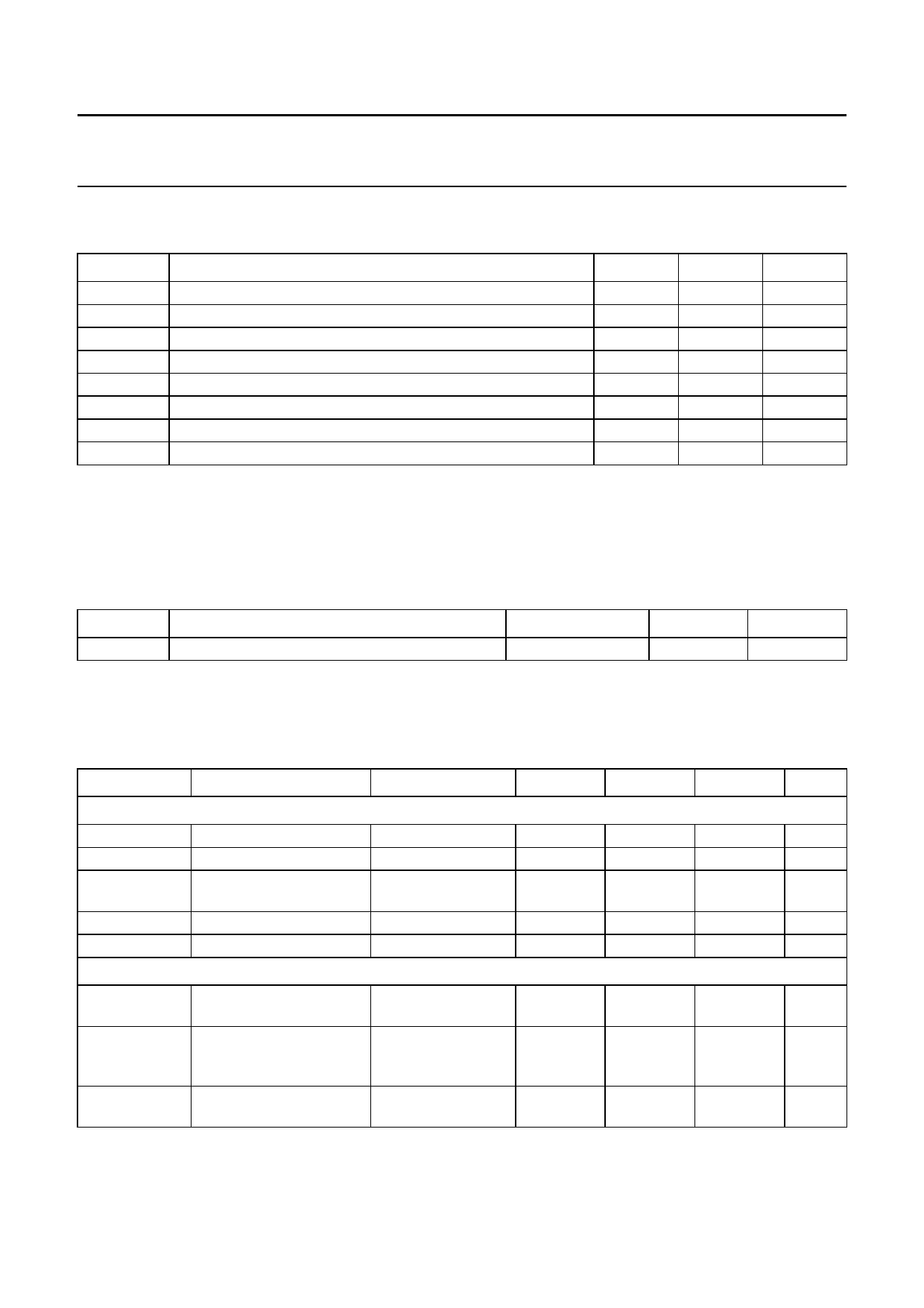
LIMITING VALUES
In accordance with the Absolute Maximum Rating System (IEC 134).
SYMBOL
VDDA
VDDD
∆VDD
VI
IO
Tstg
Tamb
Tj
PARAMETER
analog supply voltage
digital supply voltage
supply voltage difference between VDDA and VDDD
input voltage level
output current
storage temperature
ambient temperature
junction temperature
MIN.
−0.3
−0.3
−1.0
−0.3
−
−55
−40
−
MAX.
+7.0
+7.0
+4.0
+7.0
10
+150
+85
150
UNIT
V
V
V
V
mA
°C
°C
°C
HANDLING
Inputs and outputs are protected against electrostatic discharges in normal handling. However, to be totally safe, it is
desirable to take normal precautions appropriate to handling integrated circuits.
THERMAL CHARACTERISTICS
SYMBOL
PARAMETER
Rth(j-a)
thermal resistance from junction to ambient
CONDITIONS
in free air
VALUE
120
UNIT
K/W
CHARACTERISTICS
VDDA = V11 to V12 = 4.75 to 5.25 V; VDDD = V18 to V17 = 3.0 to 5.25 V; VSSA and VSSD shorted together;
Tamb = −40 to +85 °C; typical values measured at VDDA = 5.0 V; VDDD = 3.3 V and Tamb = 25 °C; unless otherwise
specified; note 1.
SYMBOL
PARAMETER
CONDITIONS
MIN.
TYP.
MAX.
UNIT
Supplies
VDDA
VDDD
∆VDD
IDDA
IDDD
analog supply voltage
digital supply voltage
voltage difference
between VDDA and VDDD
analog supply current
digital supply current
4.75
5.0
3.0
3.3
−0.2
−
−
30
−
3.0
Variable gain amplifier transfer characteristics
B−3dB
td(g)
∆td(g)
−3 dB small signal
Vo(dif)(p-p) = 0.125 V; 110
130
bandwidth
Tamb = 25 °C
group delay time
up to fi = 20 MHz; −
2.5
minimum gain;
Tamb = 25 °C
group delay difference 6 dB gain step;
−
−
Tamb = 25 °C
5.25
5.25
+2.5
36
5.0
−
−
300
V
V
V
mA
mA
MHz
ns
ps
1999 Oct 08
5
Share Link: 