TC7660 데이터 시트보기 (PDF) - TelCom Semiconductor Inc => Microchip
부품명
상세내역
일치하는 목록
TC7660 Datasheet PDF : 9 Pages
| |||
CHARGE PUMP DC-TO-DC
VOLTAGE CONVERTER
1
TC7660
C1 +
10µF
1
8
2
7
3 TC7660 6
4
5
COSC*
IS
V+
(+5V)
IL
RL
VO
C2
+ 10µF
NOTES: * For large values of COSC (>1000pF), the values
of C1 and C2 should be increased to 100µF.
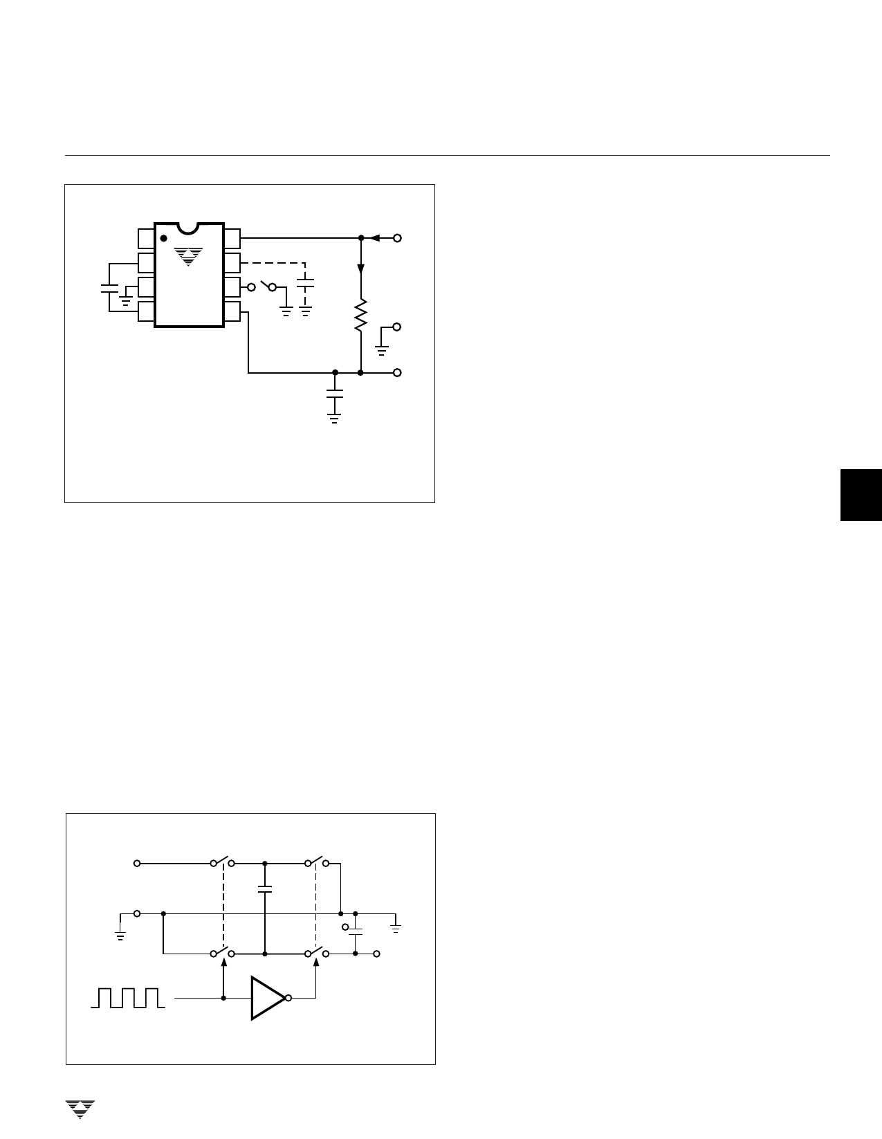
Figure 1. TC7660 Test Circuit
Detailed Description
The TC7660 contains all the necessary circuitry to
implement a voltage inverter, with the exception of two
external capacitors, which may be inexpensive 10 µF polar-
ized electrolytic capacitors. Operation is best understood by
considering Figure 2, which shows an idealized voltage
inverter. Capacitor C1 is charged to a voltage, V+, for the half
cycle when switches S1 and S3 are closed. (Note: Switches
S2 and S4 are open during this half cycle.) During the second
half cycle of operation, switches S2 and S4 are closed, with
S1 and S3 open, thereby shifting capacitor C1 negatively by
V+ volts. Charge is then transferred from C1 to C2, such that
the voltage on C2 is exactly V+, assuming ideal switches and
no load on C2.
The four switches in Figure 2 are MOS power switches;
2 S1 is a P-channel device, and S2, S3 and S4 are N-channel
devices. The main difficulty with this approach is that in
integrating the switches, the substrates of S3 and S4 must
always remain reverse-biased with respect to their sources,
but not so much as to degrade their ON resistances. In
addition, at circuit start-up, and under output short circuit
conditions (VOUT = V+), the output voltage must be sensed
and the substrate bias adjusted accordingly. Failure to
3 accomplish this will result in high power losses and probable
device latch-up.
This problem is eliminated in the TC7660 by a logic
network which senses the output voltage (VOUT) together
with the level translators, and switches the substrates of S3
and S4 to the correct level to maintain necessary reverse
bias.
The voltage regulator portion of the TC7660 is an
4 integral part of the anti-latch-up circuitry. Its inherent voltage
drop can, however, degrade operation at low voltages. To
improve low-voltage operation, the LV pin should be
connected to GND, disabling the regulator. For supply
voltages greater than 3.5V, the LV terminal must be left
open to ensure latch-up-proof operation and prevent device
damage.
Theoretical Power Efficiency
Considerations
5
In theory, a capacitive charge pump can approach
100% efficiency if certain conditions are met:
(1) The drive circuitry consumes minimal power.
(2) The output switches have extremely low ON
resistance and virtually no offset.
(3) The impedances of the pump and reservoir
capacitors are negligible at the pump frequency.
6
V+
S1
GND
S3
S2
C2
S4
VOUT
= – VIN
7
Figure 2. Idealized Charge Pump Inverter
TELCOM SEMICONDUCTOR, INC.
8
4-55
Share Link: 