TA8002 데이터 시트보기 (PDF) - Toshiba
부품명
상세내역
일치하는 목록
TA8002 Datasheet PDF : 9 Pages
| |||
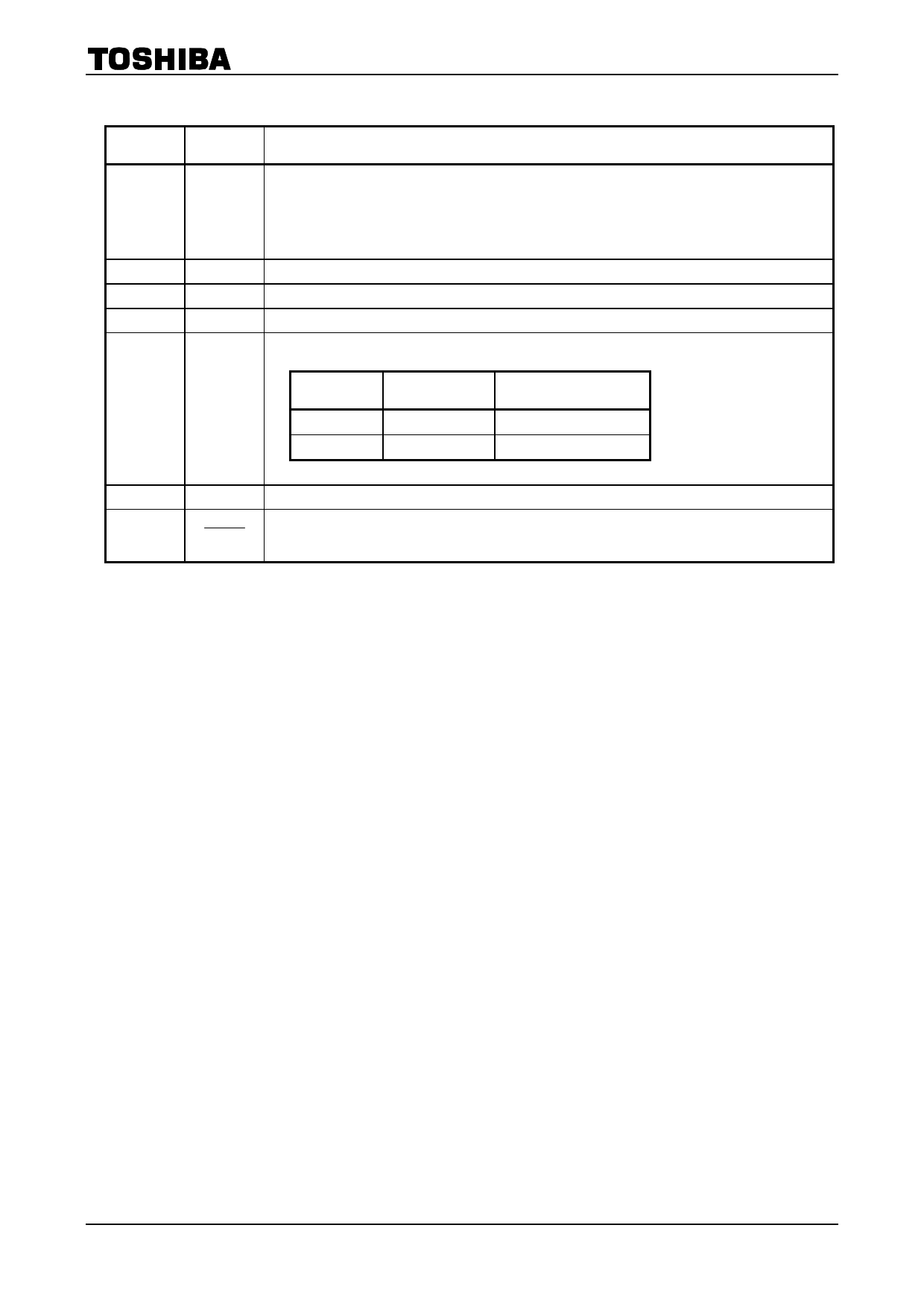
PIN DESCRIPTION
TA8002S/AS
PIN No.
1
2
3
4
5
SYMBOL
DESCRIPTION
BIAS
OUT
VCC
GND
Power supply starting pin. The starting current is supplied through a resistor to which the input voltage
is applied. The output current from this starting current is as follows :
IOUT (OUT Pin) ≥HFE× (VIN−0.7) / (200+R1) (mA)
where R1 is the external resistance attached to Bias Pin (kΩ) .
When VCC rises above 2.7V, the starting current is absorbed in the internal circuit ; instead, the
output current OUT is supplied via VCC.
Connected to the base of an external PNP transistor so that the output voltage is stabilized.
Power supply pin for internal circuit. The output voltage can also be detected at this pin.
Grounded
The output voltage can be adjusted by inserting a resistor between ADJ and GND or between ADJ
and VCC.
Mode
ADJ Pin
Output Voltage VREG
ADJ
Standby
OPEN
3.5V
Normal
GND
5.0V
6
TC
Time setting pin for reset timer. Use external RT and CT to set the time.
NPN transistor open-collector output. This pin supplies a reset signal when the output drops below
7
RESET 92% of the specified level. After the output voltage increases above 92% of the specified level, the
reset signal will be output for a period of time set at the TC pin.
2
2002-03-12
Share Link: 