STK12C68 데이터 시트보기 (PDF) - Cypress Semiconductor
부품명
상세내역
일치하는 목록
STK12C68 Datasheet PDF : 24 Pages
| |||
STK12C68
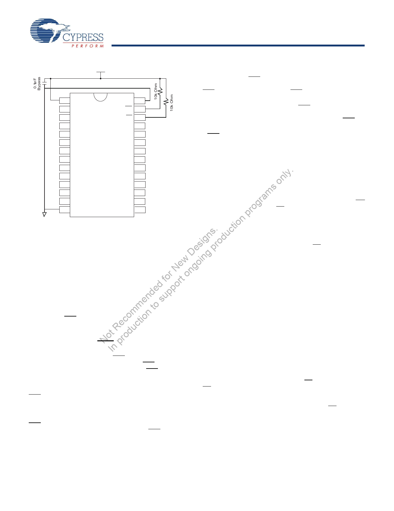
Figure 3. AutoStore Inhibit Mode
9&$3
9FF
:(
+6%
the STK12C68 continues SRAM operations for tDELAY. During
tDELAY, multiple SRAM Read operations take place. If a Write is
in progress when HSB is pulled LOW, it allows a time, tDELAY to
complete. However, any SRAM Write cycles requested after
HSB goes LOW are inhibited until HSB returns HIGH.
During any STORE operation, regardless of how it is initiated,
the STK12C68 continues to drive the HSB pin LOW, releasing it
only when the STORE is complete. After completing the STORE
operation, the STK12C68 remains disabled until the HSB pin
returns HIGH.
If HSB is not used, it is left unconnected.
Hardware RECALL (Power Up)
During power up or after any low power condition (VCC <
ograms only. 9VV
ns. uction pr If the power supply drops faster than 20 us/volt before Vcc
sig rod reaches VSWITCH, then a 2.2 ohm resistor should be connected
e p between VCC and the system supply to avoid momentary excess
D g of current between VCC and VCAP.
New goin AutoStore Inhibit Mode
for rt on If an automatic STORE on power loss is not required, then VCC
ed po is tied to ground and +5V is applied to VCAP (Figure 3). This is
d p the AutoStore Inhibit mode, where the AutoStore function is
en su disabled. If the STK12C68 is operated in this configuration, refer-
m to ences to VCC are changed to VCAP throughout this data sheet.
m n In this mode, STORE operations are triggered through software
co tio control or the HSB pin. To enable or disable Autostore using an
e c I/O port pin see Preventing Store on page 6. It is not permissible
t R du to change between these three options “on the fly”.
NoIn pro Hardware STORE (HSB) Operation
VRESET), an internal RECALL request is latched. When VCC
once again exceeds the sense voltage of VSWITCH, a RECALL
cycle is automatically initiated and takes tHRECALL to complete.
If the STK12C68 is in a Write state at the end of power up
RECALL, the SRAM data is corrupted. To help avoid this
situation, a 10 Kohm resistor is connected either between WE
and system VCC or between CE and system VCC.
Software STORE
Data is transferred from the SRAM to the nonvolatile memory by
a software address sequence. The STK12C68 software STORE
cycle is initiated by executing sequential CE controlled Read
cycles from six specific address locations in exact order. During
the STORE cycle, an erase of the previous nonvolatile data is
first performed followed by a program of the nonvolatile
elements. When a STORE cycle is initiated, input and output are
disabled until the cycle is completed.
Because a sequence of Reads from specific addresses is used
for STORE initiation, it is important that no other Read or Write
accesses intervene in the sequence. If they intervene, the
sequence is aborted and no STORE or RECALL takes place.
To initiate the software STORE cycle, the following Read
sequence is performed:
1. Read address 0x0000, Valid READ
2. Read address 0x1555, Valid READ
3. Read address 0x0AAA, Valid READ
The STK12C68 provides the HSB pin for controlling and 4. Read address 0x1FFF, Valid READ
acknowledging the STORE operations. The HSB pin is used to
request a hardware STORE cycle. When the HSB pin is driven
LOW, the STK12C68 conditionally initiates a STORE operation
after tDELAY. An actual STORE cycle only begins if a Write to the
SRAM takes place since the last STORE or RECALL cycle. The
HSB pin also acts as an open drain driver that is internally driven
LOW to indicate a busy condition, while the STORE (initiated by
any means) is in progress.
SRAM Read and Write operations, that are in progress when
HSB is driven LOW by any means, are given time to complete
5. Read address 0x10F0, Valid READ
6. Read address 0x0F0F, Initiate STORE cycle
The software sequence is clocked with CE controlled Reads or
OE controlled Reads. When the sixth address in the sequence
is entered, the STORE cycle commences and the chip is
disabled. It is important that Read cycles and not Write cycles
are used in the sequence. It is not necessary that OE is LOW for
a valid sequence. After the tSTORE cycle time is fulfilled, the
SRAM is again activated for Read and Write operation.
before the STORE operation is initiated. After HSB goes LOW,
Document Number: 001-51027 Rev. *C
Page 5 of 24
[+] Feedback
Share Link: 