MX806ADW 데이터 시트보기 (PDF) - MX-COM Inc
부품명
상세내역
일치하는 목록
MX806ADW Datasheet PDF : 23 Pages
| |||
Audio Processor
5
MX806A
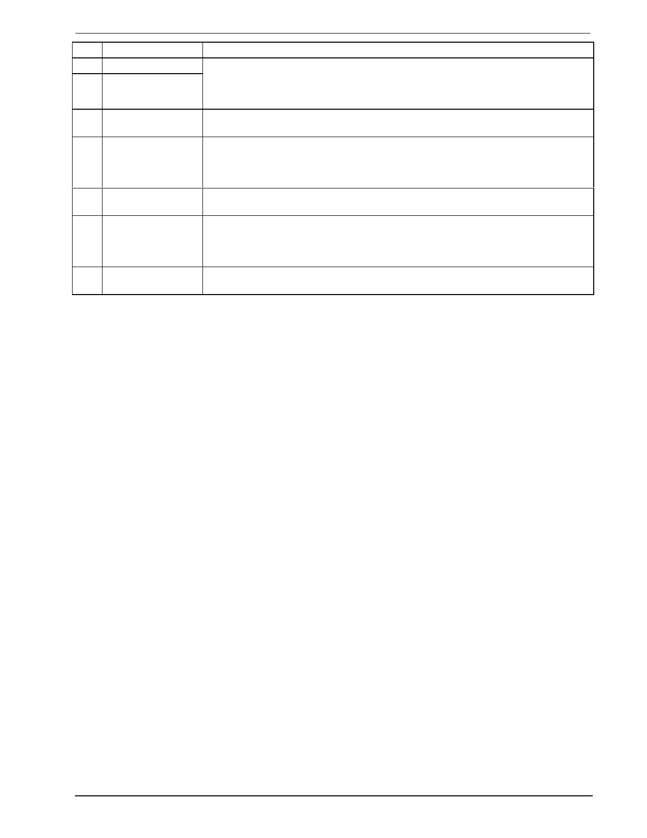
Pin
Signal
Description
18 Sum In
19 Sum Out
The input and output terminals of the on-chip Modulation Summing Amplifier.
External components are required for input signals and gain/attenuation setting as
shown in Figure 2. For single-signal, no gain requirements, Main Process Out
may be linked directly to Modulation In.
20 Modulation In
The final, composite modulating signal to VCO (Mod 1) and Reference (Mod 2)
Output Drives
21 Audio Output
The processed audio signal output intended as a received audio (volume) output.
Though normally used in the RX mode, operation in TX is permitted. The output
level of this attenuator is controlled via a Volume Set command. During
Powersave this output is placed at VSS.
22 Modulation 1 Drive The drive to the radio modulator Voltage Controlled Oscillator (VCO) from the
composite audio summing stage.
23 Modulation 2 Drive The drive to the radio modulator Reference Oscillator from the composite audio
summing stage.
Note: These VCO output attenuators are individually adjustable using the
Modulator Level command. During Powersave these outputs are placed at VSS.
24 VDD
Positive Supply. A single 5.0V regulated supply is required. Levels and voltages
within this Audio Processor are dependent upon this supply.
Table 1: Signal List
1998 MX-COM, Inc.
www.mxcom.com Tel: 800 638 5577 336 744 5050 Fax: 336 744 5054
Doc. # 20480064.006
4800 Bethania Station Road, Winston-Salem, NC 27105-1201 USA
All trademarks and service marks are held by their respective companies.
Share Link: 