NJU6680 데이터 시트보기 (PDF) - Japan Radio Corporation
부품명
상세내역
일치하는 목록
NJU6680 Datasheet PDF : 56 Pages
| |||
NJU6680
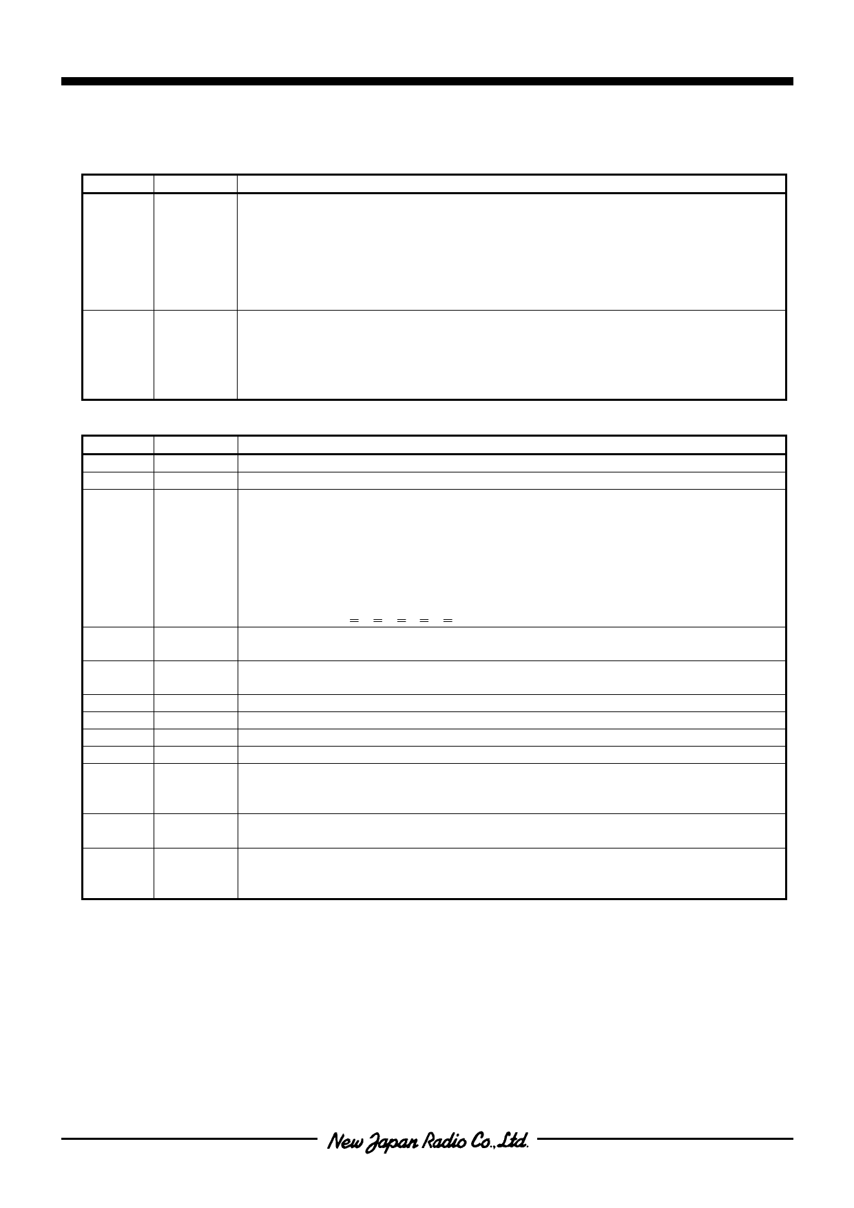
TERMINAL DESCRIPTION
• Power Supply
No.
Terminal
19-21,
VDD
27-29,
36-38,
45-48,
57-60,
71-73,
77,87
23-25,
VSS
31-33,
41-43,
62,75,
79,86
Power Supply
Ground, 0V
Description
• Internal Power Circuits
No.
Terminal
Description
61
VCI
Voltage converter input terminal
63
VOUT
Voltage converter output terminal
84
V0
LCD driving voltage terminals
83
V1
• When the internal power circuits are used, the LCD driving voltages (V0 to V4) are
82
V2
enabled by the “Power control set” instruction and an LCD bias ratio is selected by
81
V3
the “LCD bias set” instruction.
80
V4
• When the internal power circuits are not used, the external voltages (V0 to V4) are
required on these terminals. The external voltages should be maintained in the
relationship: VSS<V4<V3<V2<V1<V0.
67
C1+
Capacitor terminals for voltage converter
66
C1-
68
C2+
Capacitor terminals for voltage converter
69
C2-
65
C3+
Capacitor terminal for voltage converter
70
C4+
Capacitor terminal for voltage converter
64
C5+
Capacitor terminal for voltage converter
85
VR
V0 voltage adjustment terminal
74
REF Internal or external reference voltage select terminal
“H”: Internal
“L”: External
76
VEXT External reference voltage input terminal
• This terminal is valid when the REF terminal is connected to “L”.
78
INTRS Internal resistor select terminal
“H”: Internal
“L”: External
-8-
8
Ver.2003-04-08
Share Link: 