NJU6680 데이터 시트보기 (PDF) - Japan Radio Corporation
부품명
상세내역
일치하는 목록
NJU6680 Datasheet PDF : 56 Pages
| |||
NJU6680
Functional Description
(1) Description of each blocks
(1-1) Busy Flag (BF)
The BF is used to indicate whether the LSI is busy or not. During the busy status, the LSI cannot accept
any instruction except the “Status read” instruction, which reads out the BF through the D7 terminal. When
the cycle time (tcyc) mentioned in “AC characteristics” is satisfied, the BF is not required after each
instruction so that it is possible to improve the process performance of an MPU.
(1-2) Initial display line register
The initial display line register is used to specify the DDRAM line address corresponding to the COM0 by
the “Initial display line set” instruction. It is used not only for normal display but also vertical scrolling and
page switching displays without changing the display data in the DDRAM.
(1-3) Line Counter
The line counter is used to provide the DDRAM line address. The line address is initialized whenever
the polarity of an internal frame signal (FR) is switched, and then it is counted up in synchronization of a
common timing signal.
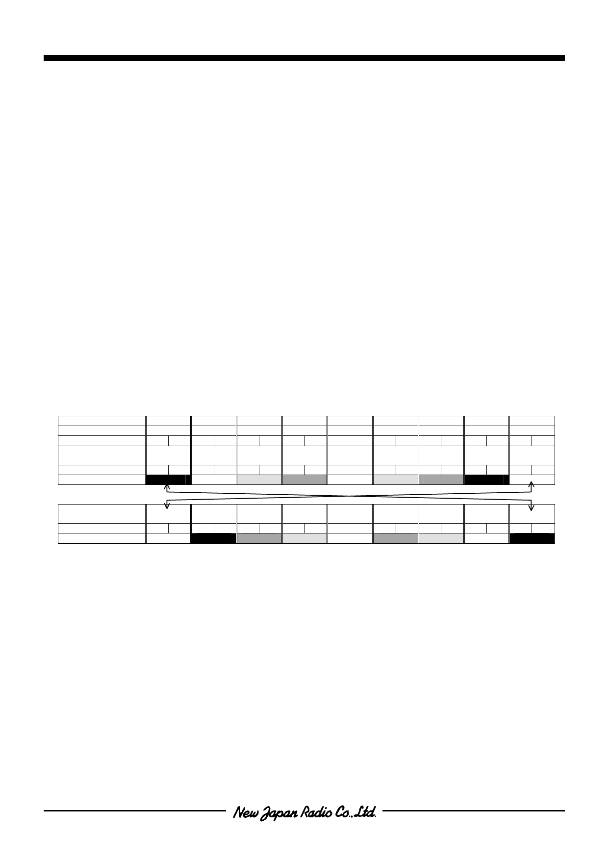
(1-4) Column Address Counter
An MPU can access only 7-bit [C6:C0] “column address” by the “Column address LSB set” and “Column
address MSB set” instructions. When both 4-bit LSB and 3-bit MSB data is set into the column address
register, 8-bit “internal column address” is established in the LSI as illustrated in the following figure, and
accordingly, 2-bit display data must be written for each pixel with two successive bytes.
The column address automatically increases by 1 (+1) after each 2-byte display data and wraps around
to the column address (00)H in the same page after the last column is addressed. The assignment of the
column address for the segment drivers can be reversed by the “ADC set” instruction.
Segment outputs
SEG0
SEG1
SEG2
SEG3
….
SEG124
SEG125
SEG126
SEG127
Internal Column address (00)H (01)H (02)H (03)H (04)H (05)H (06)H (07)H
….
(F8)H (F9)H (FA)H (FB)H (FC)H (FD)H (FE)H (FF)H
Column address
(ADC=0)
(00)H
(01)H
(02)H
(03)H
….
(7C)H
(7D)H
(7E)H
(7F)H
Display data
11000110
….
01101100
Display image
….
Column address
(ADC=1)
Display data
Display image
(7F)H
(7E)H
(7D)H
(7C)H
….
(03)H
(02)H
(01)H
(00)H
00111001
….
10010011
….
(1-5) Page Address Register
The page address register is used to provide the DD RAM page address.
(1-6) Display data RAM (DD RAM)
The Display data RAM (DD RAM) is the bit map RAM consisting of 32,768-bit to store the display data
corresponding to 128x128 pixels on LCD panel. Each LCD pixel corresponds to two bits in the display
data RAM in gray scale mode and to one bit in black & white mode, display data respectively.
The DD RAM data : "00" = Gray Scale Level 0 ( Set by the “Gray Scale Level Select” instruction)
The DD RAM data : "01" = Gray Scale Level 1 (
“
)
The DD RAM data : "10" = Gray Scale Level 2 (
“
)
The DD RAM data : "11" = Gray Scale Level 3 (
“
)
The DD RAM data and the state of the LCD in Black & White Mode:
In Normal Display : "1"=Turn-On Display, "0" =Turn-Off Display
In Reverse Display : "1"=Turn-Off Display, "0" =Turn-On Display
- 10 -
10
Ver.2003-04-08
Share Link: 