NCP690(2009) 데이터 시트보기 (PDF) - ON Semiconductor
부품명
상세내역
일치하는 목록
NCP690
(Rev.:2009)
(Rev.:2009)
ON Semiconductor

NCP690 Datasheet PDF : 14 Pages
| |||
NCP690, NCP691, NCP692
DEFINITIONS
Load Regulation
The change in output voltage for a change in output load
current at a constant temperature.
Dropout Voltage
The input/output differential at which the regulator output
no longer maintains regulation against further reductions in
input voltage. Measured, when the output drops 100 mV
below its nominal value. The junction temperature, load
current, and minimum input supply requirements affect the
dropout level.
Output Noise Voltage
This is the integrated value of the output noise over a
specified frequency range. Input voltage and output load
current are kept constant during the measurement. Results
are expressed in mVrms or nV √Hz.
Ground Current
Ground Current is the current that flows through the
ground pin when the regulator operates without a load on its
output (IGND). This consists of internal IC operation, bias,
etc. It is actually the difference between the input current
(measured through the LDO input pin) and the output load
current. If the regulator has an input pin that reduces its
internal bias and shuts off the output (enable/disable
function), this term is called the disable current (IDIS.)
Line Regulation
The change in output voltage for a change in input voltage.
The measurement is made under conditions of low
dissipation or by using pulse techniques such that the
average junction temperature is not significantly affected.
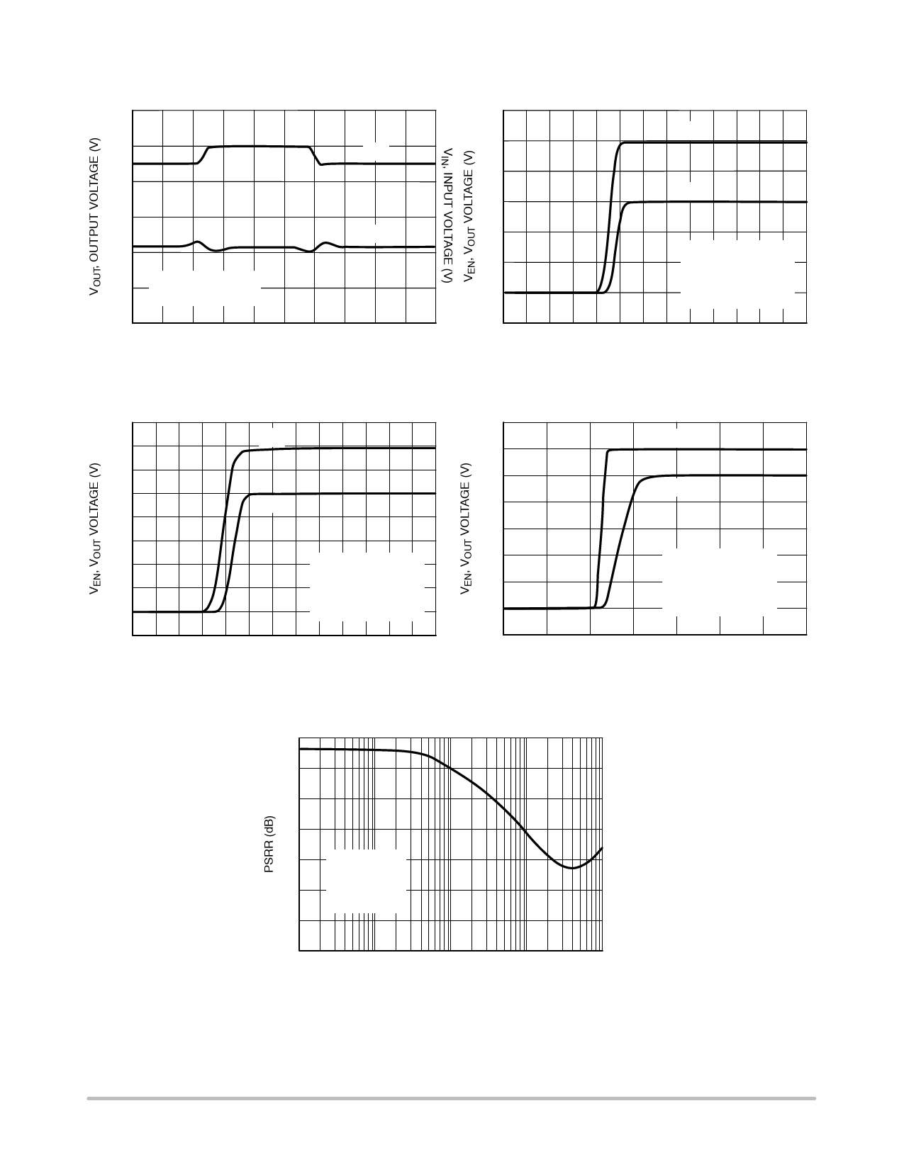
Line Transient Response
Typical output voltage overshoot and undershoot
response when the input voltage is excited with a given
slope.
Load Transient Response
Typical output voltage overshoot and undershoot
response when the output current is excited with a given
slope between no−load and full−load conditions.
Thermal Protection
Internal thermal shutdown circuitry is provided to protect
the integrated circuit in the event that the maximum junction
temperature is exceeded. When activated at typically 175°C,
the regulator turns off. This feature is provided to prevent
failures from accidental overheating.
Maximum Package Power Dissipation
The power dissipation level at which the junction
temperature reaches its maximum operating value.
APPLICATIONS INFORMATION
The NCP690 regulator is self−protected with internal
thermal shutdown and internal current limit. Typical
application circuit is shown in Figure 1.
Input Decoupling (CIN)
A ceramic 10 mF capacitor is recommended and should be
connected close to the NCP690 package. Higher
capacitance and lower ESR will improve the overall line
transient response.
Output Decoupling (COUT)
The NCP690 does not require a minimum Equivalent
Series Resistance (ESR) for the output capacitor. The
minimum output decoupling capacitor required for stability
is 1 mF. In order to improve the load transient response and
start up performance 10 mF capacitor is recommended. The
regulator is stable with ceramic chip as well as tantalum
capacitors. Larger values improve noise rejection and load
transient response.
No−Load Regulation Considerations
The required minimum 100 mA load current is assured by
the internal resistor divider network.
The NCP690 contain an overshoot clamp circuit to
improve transient response during a load current step
release. When output voltage exceeds the nominal by
approximately 20 mV, this circuit becomes active and
clamps the output from further voltage increase. Tying the
ENABLE pin to VIN will ensure that the part is active
whenever the supply voltage is present,
Noise Decoupling
The NCP690 is a low noise regulator and needs no
external noise reduction capacitor. Unlike other low noise
regulators which require an external capacitor and have slow
startup times, the NCP690 operates without a noise
reduction capacitor, has a typical 50 ms turn−on time and
achieves a 50 mVrms overall noise level between 10 Hz and
100 kHz.
Enable Operation
The enable pin will turn the regulator on or off. The
threshold limits are covered in the electrical characteristics
table in this data sheet. The turn−on/turn−off transient
voltage being supplied to the enable pin should exceed a
slew rate of 10 mV/ms to ensure correct operation. If the
enable function is not to be used then the pin should be
connected to VIN.
Adjustable Operation
The output voltage can be adjusted from 1 to 4 times the
typical 1.250 V regulation voltage by the use of resistor
http://onsemi.com
11
Share Link: