NCP606 데이터 시트보기 (PDF) - ON Semiconductor
부품명
상세내역
일치하는 목록
NCP606 Datasheet PDF : 14 Pages
| |||
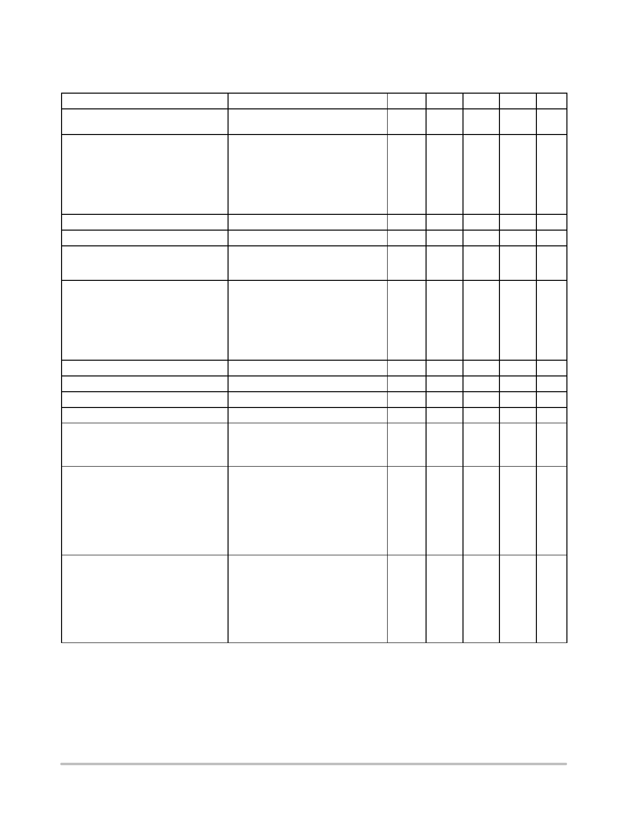
NCP605, NCP606
ELECTRICAL CHARACTERISTICS
Vin = (Vout + 0.5 V) or 1.5 V, whichever is higher, Cin = 1 mF, Cout = 1 mF, for typical values TA = 25°C, for min/max values TA = −40°C to
85°C; unless otherwise noted. (Notes 9 and 10)
Parameter
Test Conditions
Symbol Min
Typ
Max Unit
Output voltage (Adjustable Version)
Output voltage (Fixed Versions)
Vin = 1.75 V to 6 V
Iout = 1 mA to 500 mA
1.5 V
1.8 V
2.5 V
2.8 V
3.0 V
3.3 V
5.0 V
Vin = (Vout + 0.5 V) to 6 V
Iout = 1 mA to 500 mA
Vout
1.231 1.250 1.269
V
(−1.5%)
(+1.5%)
Vout
1.470
1.5
1.530
V
1.764 1.8 1.836
2.450 2.5 2.550
2.744 2.8 2.856
2.940 3.0 3.060
3.234 3.3 3.366
4.900 5.0 5.100
(−2%)
(+2%)
Line regulation
Vin = (Vout + 0.5 V) to 6 V, Iout = 1 mA
Load regulation
Iout = 1 mA to 500 mA
Dropout voltage (Adjustable Version)
(Note 9)
VDO = Vin − Vout
Vout = 1.25 V
Iout = 500 mA
Dropout voltage (Fixed Version)
1.5 V
1.8 V
2.5 V
2.8 V
3.0 V
3.3 V
5.0 V
VDO = Vin − (Vout − 0.1 V)
Iout = 500 mA
Vout = 0 V to 90% Vout(nom)
Regline
−
Regload
−
VDO
−
VDO
−
−
−
−
−
−
−
4
10
mV
10
30
mV
mV
450
470
mV
290
360
250
300
200
250
190
240
180
230
170
220
150
200
Disable Current (NCP606 Only) (Note 10)
Ground Current
Current Limit (Note 11)
Output Short Circuit Current
Enable Input Threshold Voltage
(NCP606 Only)
Voltage Increasing, Logic High
Voltage Decreasing, Logic Low
VEN = 0 V
Iout = 1 mA to 500 mA
Vout = Vout(nom) − 10 %
Vout = 0 V
High
Low
IDIS
−
IGND
−
ILIM
675
ISC
700
Vth(EN)
0.9
−
0.1
1
mA
145
180
mA
−
−
mA
1000 1350 mA
V
−
−
−
0.4
Turn−on Time (Note 11)
1.25 V
1.5 V
1.8 V
2.5 V
2.8 V
3.0 V
3.3 V
5.0 V
Vin = 0 V to (Vout + 0.5 V) or 1.75 V,
whichever is higher
Vout = 0 V to 90% of Vout(nom)
ton
ms
−
6
−
−
6
−
−
7
−
−
8
−
−
10
−
−
12
−
−
15
−
−
30
−
Enable Time (NCP606 Only) (Note 11)
1.25 V
1.5 V
1.8 V
2.5 V
2.8 V
3.0 V
3.3 V
5.0 V
VEN = From 0 V to Vin
tEN
ms
−
12
−
−
12
−
−
13
−
−
16
−
−
18
−
−
19
−
−
20
−
−
30
−
7. Refer to ABSOLUTE MAXIMUM RATINGS and APPLICATION INFORMATION for Safe Operating Area.
8. Performance guaranteed over the indicated operating temperature range by design and/or characterization tested at TJ = TA = 25°C. Low
duty cycle pulse techniques are used during testing to maintain the junction temperature as close to ambient as possible.
9. Maximum dropout voltage is limited to minimum input voltage Vin = 1.7 V recommended for guaranteed operation at maximum output
current.
10. Refer to application information section.
11. Values based on design and/or characterization.
http://onsemi.com
4
Share Link: 