NCP348 데이터 시트보기 (PDF) - ON Semiconductor
부품명
상세내역
일치하는 목록
NCP348 Datasheet PDF : 13 Pages
| |||
NCP348, NCP348AE
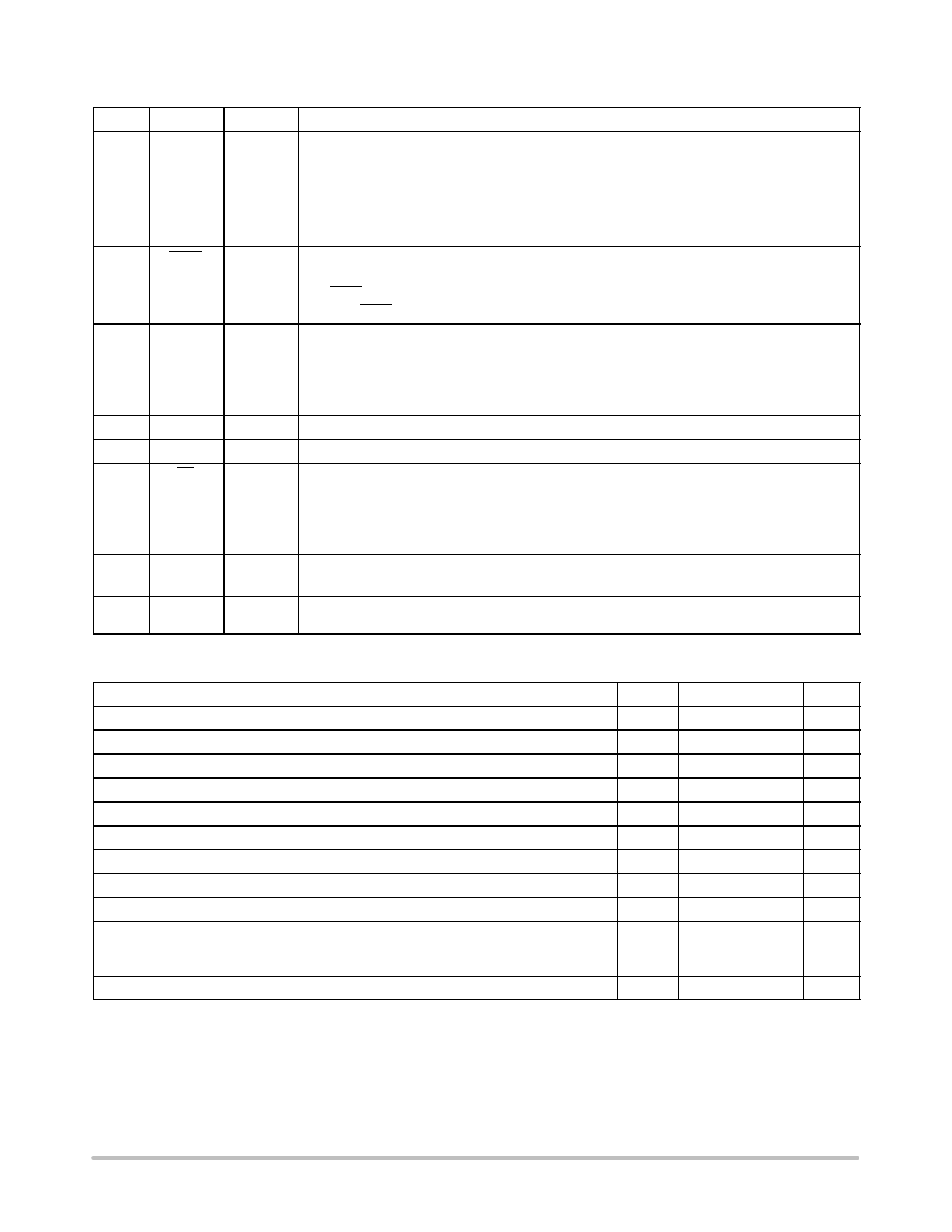
PIN FUNCTION DESCRIPTION
Pin No. Symbol Function
Description
1
IN
POWER Input Voltage Pin.
4
This pin is connected to the power supply.
5
The device system core is supplied by this input.
A 1 mF low ESR ceramic capacitor, or larger, must be connected between this pin and GND.
The three IN pins must be hardwired to common supply.
2
GND
POWER Ground
3
FLAG
OUTPUT Fault Indication Pin.
This pin allows an external system to detect a fault on IN pin.
The FLAG pin goes low when input voltage exceeds OVLO threshold or drop below UVLO threshold.
Since the FLAG pin is open drain functionality, an external pull up resistor to VCC must be added.
6
OUT
OUTPUT Output Voltage Pin.
7
This pin follows IN pin when “no fault” is detected.
The output is disconnected from the Vin power supply when the input voltage is under the UVLO
threshold or above OVLO threshold.
The two OUT pins must be hardwired to common supply.
8
NC
OPEN No Connect
9
NC
OPEN No Connect
10
EN
INPUT Enable Pin.
The device enters in shutdown mode when this pin is tied to a high level. In this case the output is
disconnected from the input.
To allow normal functionality, the EN pin shall be connected to GND to a pull down or to a I/O pin.
This pin does not have an impact on the fault detection.
PAD1
PAD1, under the device. See PCB recommendations page 10.
Can be shorted to GND.
PAD2
The PAD2 is electrically connected to the internal NMOS drain and connected to Pins 4 and 5.
See PCB recommendations page 10.
MAXIMUM RATINGS
Rating
Symbol
Value
Unit
Minimum Voltage (IN to GND)
Minimum Voltage (All others to GND)
Vminin
−0.3
V
Vmin
−0.3
V
Maximum Voltage (IN to GND)
Maximum Voltage (All others to GND)
Vmaxin
30
V
Vmax
7.0
V
Maximum Current (UVLO<VIN<OVLO)
Thermal Resistance, Junction−to−Air (Note 1)
Operating Ambient Temperature Range
Storage Temperature Range
Junction Operating Temperature
ESD Withstand Voltage (IEC 61000−4−2) (input only) when bypassed with 1.0 mF capacitor
Human Body Model (HBM), Model = 2 (Note 2)
Machine Model (MM) Model = B (Note 3)
Imax
RqJA
TA
Tstg
TJ
Vesd
2.0
280
−40 to +85
−65 to +150
150
15 Air, 8.0 Contact
2000
200
A
°C/W
°C
°C
°C
kV
V
V
Moisture Sensitivity
MSL
Level 1
−
Stresses exceeding Maximum Ratings may damage the device. Maximum Ratings are stress ratings only. Functional operation above the
Recommended Operating Conditions is not implied. Extended exposure to stresses above the Recommended Operating Conditions may affect
device reliability.
1. The RqJA is highly dependent on the PCB heat sink area (connected to pad 2). As example RqJA is 268 °C/W with 30 mm2 (copper 35 mm) and
189 °C/W with 400 mm2.
2. Human Body Model, 100 pF discharged through a 1.5 kW resistor following specification JESD22/A114.
3. Machine Model, 200 pF discharged through all pins following specification JESD22/A115.
http://onsemi.com
3
Share Link: 