NB2309A(2015) 데이터 시트보기 (PDF) - ON Semiconductor
부품명
상세내역
일치하는 목록
NB2309A Datasheet PDF : 9 Pages
| |||
NB2309A
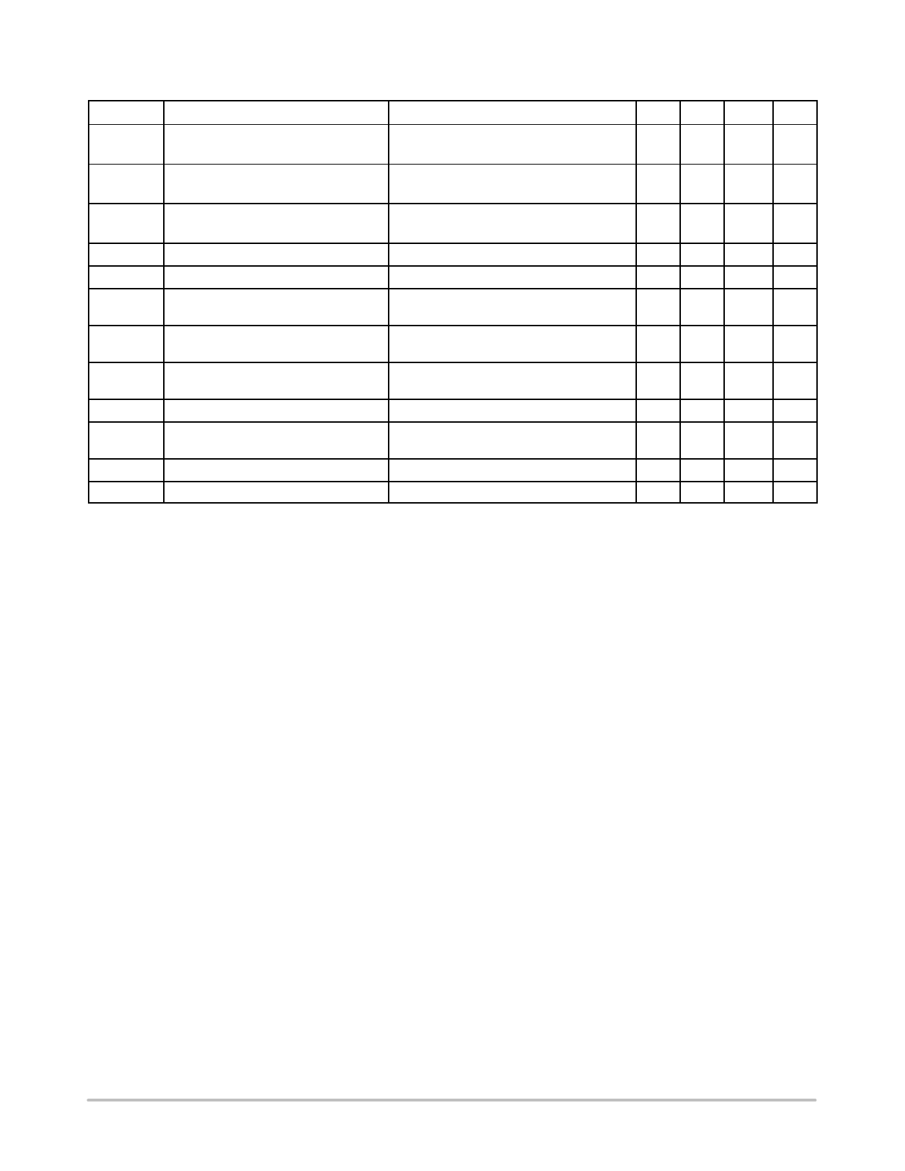
Table 6. SWITCHING CHARACTERISTICS VCC = 3.0 V to 3.6 V, GND = 0 V, TA = −40°C to +85°C (Note 6)
Parameter
Description
Test Conditions
Min Typ
1/t1
Output Frequency
30 pF load
15
10 pF load
15
1/t1
Duty Cycle = (t2 / t1) * 100 (−1, −1H) Measured at 1.4 V, FOUT = 66.67 MHz
40
50
(−1H)
< 50 MHz
45
50
t3
Output Rise Time
(−1)
Measured between 0.8 V and 2.0 V
(−1H)
t4
Output Fall Time
Measured between 2.0 V and 0.8 V
t5
Output−to−Output Skew
All outputs equally loaded
t6
Delay, REF Rising Edge to CLKOUT
Measured at VDD/2
0
Rising Edge
t7
Device−to−Device Skew
Measured at VDD/2 on the CLKOUT pins of
0
the device
t8
Output Slew Rate
Measured between 0.8 V and 2.0 V using
1
Test Circuit #2
tJ
Cycle−to−Cycle Jitter
Measured at 66.67 MHz, loaded outputs
tLOCK
PLL Lock Time
Stable power supply, valid clock presented
on REF pin
6. All parameters specified with loaded outputs in PLL−Mode.
Max
100
133
60
55
2.5
1.5
1.5
250
±350
Unit
MHz
%
ns
ns
ps
ps
700 ps
V/ns
200 ps
1.0 ms
www.onsemi.com
5
Share Link: 