NB2309A(2015) 데이터 시트보기 (PDF) - ON Semiconductor
부품명
상세내역
일치하는 목록
NB2309A Datasheet PDF : 9 Pages
| |||
NB2309A
3.3 V Zero Delay
Clock Buffer
The NB2309A is a versatile, 3.3 V zero delay buffer designed to
distribute high−speed clocks. It accepts one reference input and drives
out nine low−skew clocks. It is available in a 16 pin package.
The −1H version of the NB2309A operates at up to 133 MHz, and
has higher drive than the −1 devices. All parts have on−chip PLL’s that
lock to an input clock on the REF pin. The PLL feedback is on−chip
and is obtained from the CLKOUT pad.
The NB2309A has two banks of four outputs each, which can be
controlled by the Select inputs as shown in the Select Input Decoding
Table. If all the output clocks are not required, Bank B can be
three−stated. The select inputs also allow the input clock to be directly
applied to the outputs for chip and system testing purposes.
Multiple NB2309A devices can accept the same input clock and
distribute it. In this case the skew between the outputs of the two
devices is guaranteed to be less than 700 ps.
All outputs have less than 200 ps of cycle−to−cycle jitter. The input
and output propagation delay is guaranteed to be less than 350 ps, and
the output to output skew is guaranteed to be less than 250 ps.
The NB2309A is available in two different configurations, as shown
in the ordering information table. The NB2309A1 is the base part. The
NB2309AI1H is the high drive version of the −1 and its rise and fall
times are much faster than −1 part.
Features
• 15 MHz to 133 MHz Operating Range, Compatible with CPU and
PCI Bus Frequencies
• Zero Input − Output Propagation Delay
• Multiple Low−Skew Outputs
• Output−Output Skew Less than 250 ps
• Device−Device Skew Less than 700 ps
• One Input Drives 9 Outputs, Grouped as 4 + 4 + 1
• Less than 200 ps Cycle−to−Cycle Jitter is Compatible with PentiumR
Based Systems
• Test Mode to Bypass PLL
• Accepts Spread Spectrum Clock at the Input
• Available in 16 Pin, 150 mil SOIC and 4.4 mm TSSOP
• 3.3 V Operation, Advanced 0.35 m CMOS Technology
• Guaranteed Across Commercial and Industrial Temperature Ranges
• These are Pb−Free Devices
www.onsemi.com
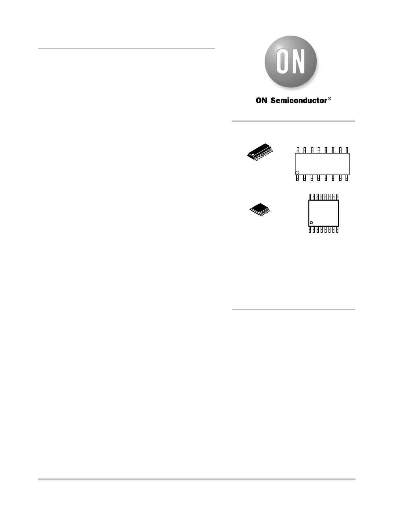
MARKING
DIAGRAMS*
16
1
SOIC−16
D SUFFIX
CASE 751B
16
1
TSSOP−16
DT SUFFIX
CASE 948F
16
XXXXXXXXG
AWLYWW
1
16
XXXX
XXXX
ALYWG
G
1
XXXX = Device Code
A
= Assembly Location
WL, L = Wafer Lot
Y
= Year
W, WW = Work Week
G or G = Pb−Free Package
(Note: Microdot may be in either location)
*For additional marking information, refer to
Application Note AND8002/D.
ORDERING INFORMATION
See detailed ordering, marking and shipping information in the
package dimensions section on page 7 of this data sheet.
© Semiconductor Components Industries, LLC, 2015
1
May, 2015 − Rev. 11
Publication Order Number:
NB2309A/D
Share Link: 